UT62L25716BS-70LLE 데이터 시트보기 (PDF) - Utron Technology Inc
부품명
상세내역
일치하는 목록
UT62L25716BS-70LLE Datasheet PDF : 10 Pages
| |||
Rev. 1.0
UTRON
UT62L25716
256K X 16 BIT LOW POWER CMOS SRAM
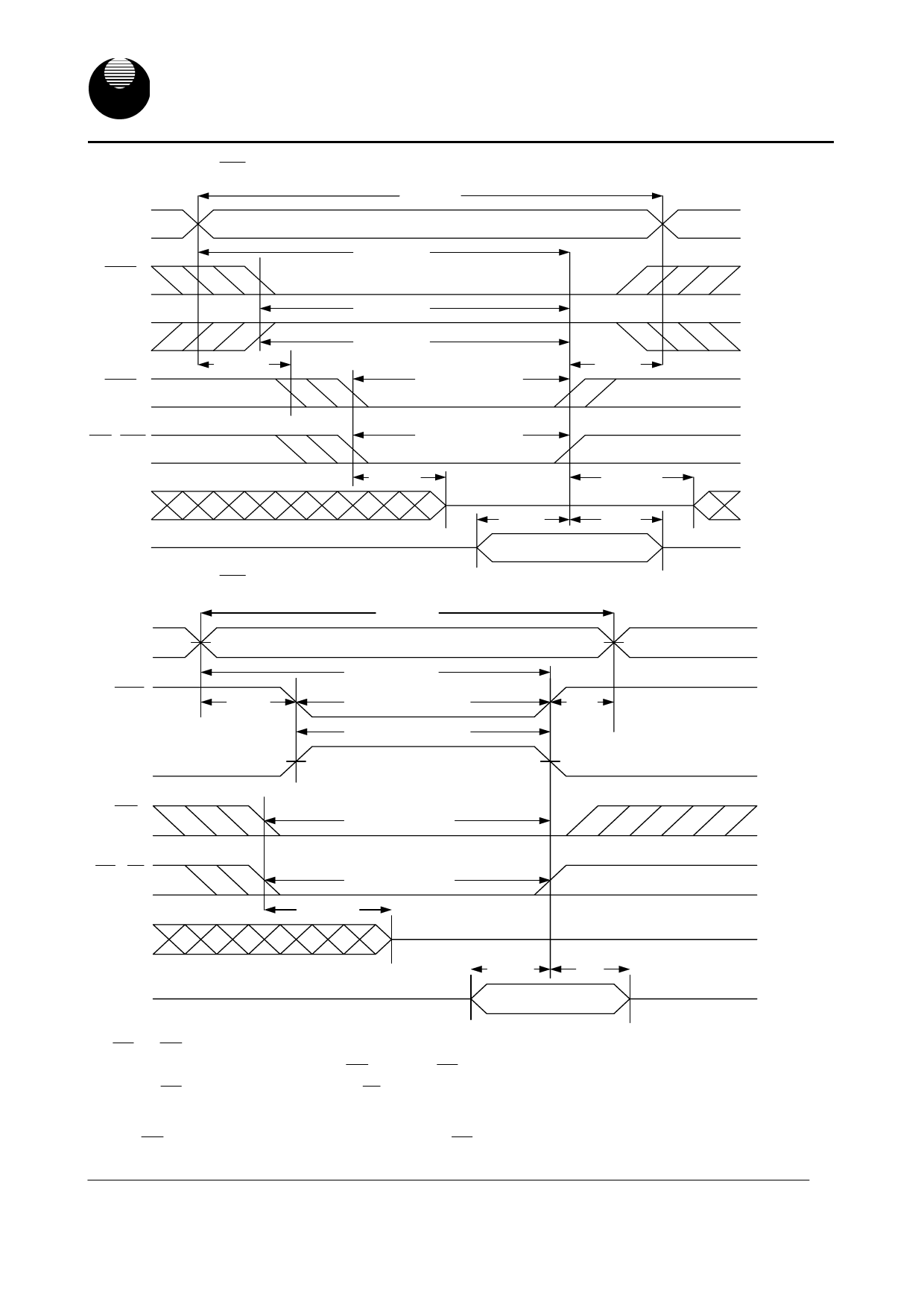
WRITE CYCLE 1 ( WE Controlled) (1,2,3,5)
t WC
Address
CE1
CE2
t AS
WE
t AW
t CW1
t CW2
t WP
t WR
LB , UB
Dout
Din
t PWB
t WH
(4)
High-Z
t DW
t OW
(4)
t DH
Data Valid
WRITE CYCLE 2 ( CE1and CE2 Controlled) (1,2,5)
t WC
Address
CE1
t AS
CE2
t AW
t CW1
t CW2
t WR
WE
t WP
LB , UB
Dout
t WHZ
t PWB
High-Z
t DW
t DH
Din
Data Valid
Notes :
1. WE or CE1 must be HIGH during all address transitions.
2. A write occurs during the overlap of a low CE1 and a low WE .
3. During a WE controlled with write cycle with OE LOW, tWP must be greater than tWHZ+tDW to allow the drivers to turn off and data to
be placed on the bus.
4. During this period, I/O pins are in the output state, and input singals must not be applied.
5. If the CE1 LOW transition occurs simultaneously with or after WE LOW transition, the outputs remain in a high impedance state.
6. tOW and tWHZ are specified with CL = 5pF. Transition is measured ± 500mV from steady state.
UTRON TECHNOLOGY INC.
1F, No. 11, R&D Rd. II, Science-Based Industrial Park, Hsinchu, Taiwan, R. O. C.
TEL: 886-3-5777882 FAX: 886-3-5777919
5
P80047
Share Link: 