CS8321 데이터 시트보기 (PDF) - Cherry semiconductor
부품명
상세내역
일치하는 목록
CS8321 Datasheet PDF : 6 Pages
| |||
Electrical Characteristics: 6V < VIN < 26V, IOUT=1mA, -40¡C ² TA ² 125¡C, -40¡C ² TJ ² 150¡C unless otherwise specified.
PARAMETER
TEST CONDITIONS
MIN
TYP
MAX
UNIT
s Output Stage
Output Voltage, VOUT
9V < VIN < 16V,
100µA ² IOUT ² 150mA
4.90
5.00
Dropout Voltage (VIN-VOUT) IOUT = 150mA, -40¡C ² TA ² 85¡C
0.3
IOUT = 150mA, TA = 125¡C
Quiescent Current, (IQ)
IOUT = 1mA @ VIN = 13V
IOUT < 50mA @ VIN = 13V
4
IOUT < 150mA @ VIN = 13V
15
Load Regulation
VIN = 14V, 100µA < IOUT < 150mA
5
Line Regulation
6V < V < 26V, IOUT = 1mA
5
Ripple Rejection
7 Ð VIN Ð 17V, IOUT = 150mA,
f = 120Hz
60
75
Current Limit
175
250
Short Circuit Output Current VOUT = 0V
Reverse Current
VOUT = 5V, VIN = 0V
60
200
140
5.10
V
0.5
V
0.6
V
200
µA
6
mA
25
mA
50
mV
50
mV
dB
mA
mA
200
µA
PACKAGE LEAD #
3L D2PAK
3L TO-220
1
1
2
2
3
3
Package Lead Description
LEAD SYMBOL
FUNCTION
VIN
Gnd
VOUT
Input Voltage
Ground. All Gnd leads must be connected to Ground.
5V, ±2%, 150mA Output.
Circuit Description and Application Notes
Voltage Reference and Output Circuitry
The CS8321 is a series pass voltage regulator. It consists of
an error amplifier, bandgap voltage reference, PNP pass
transistor with antisaturation control, and current limit.
As the voltage at the input, VIN, is increased, QN is for-
ward biased via R. QN provides base drive for QP. As QP
becomes forward biased, the output voltage, VOUT, begins
to rise as QPÕs output current charges the output capacitor.
Once VOUT rises to a certain level, the error amplifier
becomes biased and provides the appropriate amount of
base current to QP. The error amplifier monitors the scaled
output voltage via an internal voltage divider, R1 and R2,
and compares it to the bandgap voltage reference. The
error amplifierÕs output is a current which is equal to the
error amplifierÕs differential input voltage times its
transconductance. Therefore, the error amplifier varies the
base drive current to QN, which provides bias to QP, based
on the difference between the reference voltage and the
scaled output voltage, VOUT.
Antisaturation Protection
An antisaturation control circuit has also been added to
prevent the pass transistor from going into deep satura-
tion, which would cause excessive power dissipation due
to large bias currents lost to the substrate via a parasitic
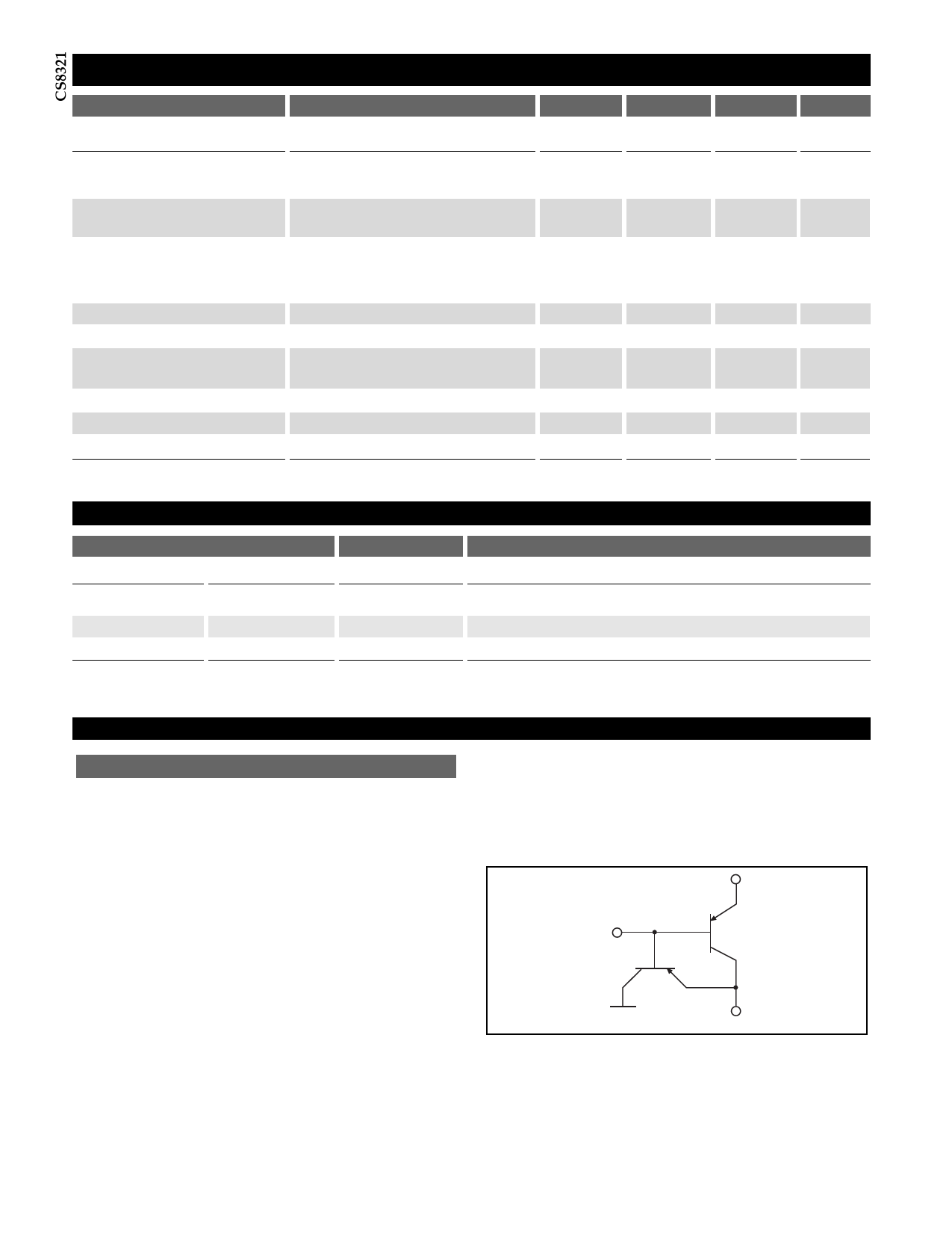
PNP transistor, as shown in Figure 1.
VIN
QP
QParasitic
Substrate
VOUT
Figure 1. The parasitic PNP transistor which is part of the pass transis-
tor (QP) structure.
2
Share Link: 