ICM7555 데이터 시트보기 (PDF) - Renesas Electronics
부품명
상세내역
일치하는 목록
ICM7555 Datasheet PDF : 13 Pages
| |||
ICM7555, ICM7556
Absolute Maximum Ratings
Supply Voltage . . . . . . . . . . . . . . . . . . . . . . . . . . . . . . . . . . . . . . . . . . . . . +18V
Input Voltage
Trigger, Control Voltage, Threshold,
Reset (Note 4). . . . . . . . . . . . . . . . . . . . . . . . . . . . . V+ +0.3V to GND -0.3V
Output Current . . . . . . . . . . . . . . . . . . . . . . . . . . . . . . . . . . . . . . . . . . . 100mA
ESD Rating
Human Body Model . . . . . . . . . . . . . . . . . . . . . . . . . . . . . . . . . . . . . . . . 2kV
Charged Device Model . . . . . . . . . . . . . . . . . . . . . . . . . . . . . . . . . . . . 100V
Operating Conditions
Temperature Range
ICM7555C . . . . . . . . . . . . . . . . . . . . . . . . . . . . . . . . . . . . . . . 0°C to +70°C
ICM7555I, ICM7556I . . . . . . . . . . . . . . . . . . . . . . . . . . . . -25°C to +85°C
Thermal Information
Thermal Resistance (Typical, Notes 5, 6) θJA (°C/W) θJC (°C/W)
14 Ld PDIP Package* . . . . . . . . . . . . . . . . 115
46
8 Ld PDIP Package* . . . . . . . . . . . . . . . . . 130
69
8 Ld SOIC Package. . . . . . . . . . . . . . . . . . . 170
67
Maximum Junction Temperature (Hermetic Package) . . . . . . . . . . . .+175°C
Maximum Junction Temperature (Plastic Package) . . . . . . . . . . . .+150°C
Maximum Storage Temperature Range . . . . . . . . . . . . . -65°C to +150°C
* Pb-free PDIPs can be used for through-hole wave solder
processing only. They are not intended for use in Reflow solder
processing applications.
CAUTION: Do not operate at or near the maximum ratings listed for extended periods of time. Exposure to such conditions may adversely impact product
reliability and result in failures not covered by warranty.
NOTES:
4. Due to the SCR structure inherent in the CMOS process used to fabricate these devices, connecting any terminal to a voltage greater than V+ +0.3V
or less than V- -0.3V may cause destructive latch-up. For this reason it is recommended that no inputs from external sources not operating from the
same power supply be applied to the device before its power supply is established. In multiple supply systems, the supply of the ICM7555 and
ICM7556 must be turned on first.
5. θJA is measured with the component mounted on a low effective thermal conductivity test board in free air. See Tech Brief TB379 for details.
6. For θJC, the “case temp” location is taken at the package top center.
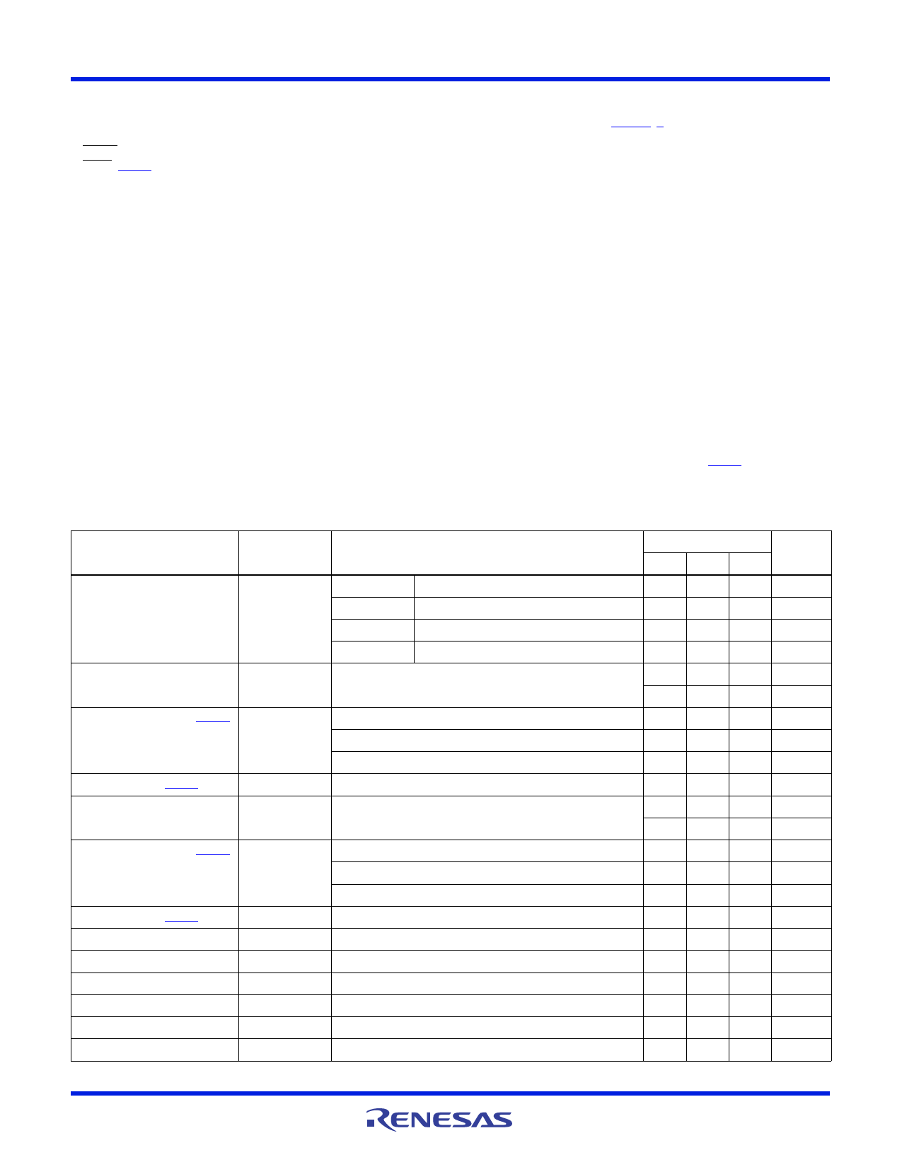
Electrical Specifications Applies to ICM7555 and ICM7556, unless otherwise specified.
PARAMETER
Static Supply Current
Monostable Timing Accuracy
SYMBOL
IDD
TEST CONDITIONS
ICM7555
VDD = 5V
VDD = 15V
ICM7556
VDD = 5V
VDD = 15V
RA = 10k, C = 0.1µF, VDD = 5V
Drift with Temperature (Note 7)
Drift with Supply (Note 7)
Astable Timing Accuracy
VDD = 5V
VDD = 10V
VDD = 15V
VDD = 5V to 15V
RA = RB = 10k, C = 0.1µF, VDD = 5V
Drift with Temperature (Note 7)
Drift with Supply (Note 7)
Threshold Voltage
Trigger Voltage
Trigger Current
Threshold Current
Control Voltage
Reset Voltage
VTH
VTRIG
ITRIG
ITH
VCV
VRST
VDD = 5V
VDD = 10V
VDD = 15V
VDD = 5V to 15V
VDD = 15V
VDD = 15V
VDD = 15V
VDD = 15V
VDD = 15V
VDD = 2V to 15V
TA = +25°C
MIN TYP MAX
40 200
60 300
80 400
120 600
2
0.5
2
0.5
62 67 71
28 32 36
10
10
62 67 71
0.4
1.0
UNIT
µA
µA
µA
µA
%
µs
ppm/°C
ppm/°C
ppm/°C
%/V
%
µs
ppm/°C
ppm/°C
ppm/°C
%/V
% VDD
% VDD
nA
nA
% VDD
V
FN2867 Rev.10.01
Mar 5, 2020
Page 3 of 13
Share Link: 