74HCT7540 데이터 시트보기 (PDF) - Nexperia B.V. All rights reserved
부품명
상세내역
일치하는 목록
74HCT7540
Nexperia B.V. All rights reserved

74HCT7540 Datasheet PDF : 15 Pages
| |||
Nexperia
74HC7540; 74HCT7540
Octal Schmitt trigger buffer/line driver; 3-state; inverting
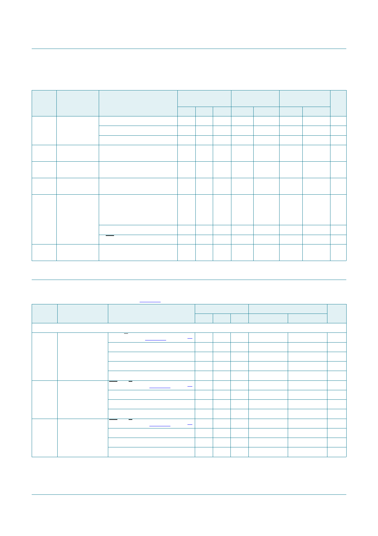
Table 6. Static characteristics …continued
At recommended operating conditions; voltages are referenced to GND (ground = 0 V).
Symbol Parameter Conditions
Tamb = 25 C
Tamb = 40 C
to +85 C
Min Typ Max Min Max
VOL
LOW-level
VI = VT+ or VT; VCC = 4.5 V
output voltage IO = 20 A;
-
0 0.1
-
IO = 6.0 mA;
- 0.15 0.26 -
II
input leakage VI = VCC or GND; VCC = 5.5 V -
- 0.1 -
current
0.1
0.33
1.0
IOZ
OFF-state
VI = VT+ or VT; VCC = 5.5 V;
-
- 0.5 -
output current VO = VCC or GND
ICC
supply current VI = VCC or GND; IO = 0 A;
-
- 8.0
-
VCC = 5.5 V
ICC
additional
supply current
per input pin; IO = 0 A;
VI = VCC 2.1 V;
other inputs at VCC or GND;
VCC = 4.5 V to 5.5 V
An input
- 20 72
-
5.0
80
90
OEn input
- 130 468 -
585
CI
input
capacitance
- 3.5 -
-
-
Tamb = 40 C
to +125 C
Min
Max
Unit
-
0.1 V
-
0.4 V
-
1.0 A
-
10 A
-
160 A
-
98 A
-
637 A
-
-
pF
10. Dynamic characteristics
Table 7. Dynamic characteristics
GND = 0 V; CL = 50 pF; for test circuit see Figure 7.
Symbol Parameter
Conditions
74HC7540
tpd
propagation delay An to Yn; see Figure 5
VCC = 2.0 V
VCC = 4.5 V
VCC = 5.0 V; CL = 15 pF
VCC = 6.0 V
ten
enable time
OEn to Yn; see Figure 6
VCC = 2.0 V
VCC = 4.5 V
VCC = 6.0 V
tdis
disable time
OEn to Yn; see Figure 6
VCC = 2.0 V
VCC = 4.5 V
VCC = 6.0 V
Tamb = 25 C
Tamb = 40 C to +125 C Unit
Min Typ Max Max (85 C) Max (125 C)
[1]
- 39 120
150
- 14 24
30
- 11 -
-
- 11 20
26
[1]
- 41 150
190
- 15 30
38
- 12 26
33
[1]
- 52 150
190
- 19 30
38
- 15 26
33
180
ns
36
ns
-
ns
31
ns
225
ns
45
ns
38
ns
225
ns
45
ns
38
ns
74HC_HCT7540
Product data sheet
All information provided in this document is subject to legal disclaimers.
Rev. 5 — 26 May 2016
© Nexperia B.V. 2017. All rights reserved
5 of 15
Share Link: