ISL8484 데이터 시트보기 (PDF) - Renesas Electronics
부품명
상세내역
일치하는 목록
ISL8484
Renesas Electronics

ISL8484 Datasheet PDF : 13 Pages
| |||
ISL8484
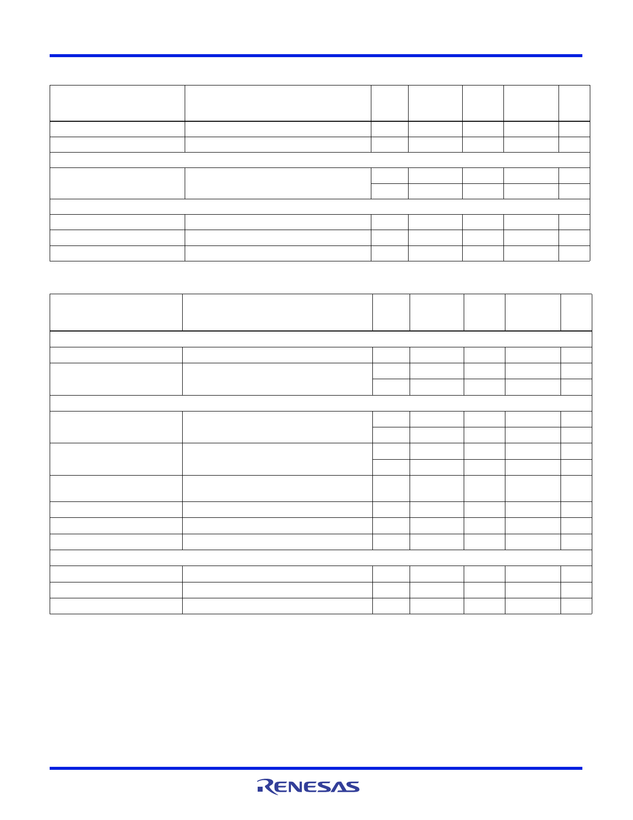
Electrical Specifications - 3V Supply
Test Conditions: V+ = +2.7V to +3.3V, GND = 0V, VINH = 1.4V, VINL = 0.5V (Note 6),
Unless otherwise specified. (Continued)
PARAMETER
TEST CONDITIONS
NO or NC OFF Capacitance, COFF f = 1MHz, VNO or VNC = VCOM = 0V (Figure 7)
COM ON Capacitance, CCOM(ON) f = 1MHz, VNO or VNC = VCOM = 0V (Figure 7)
POWER SUPPLY CHARACTERISTICS
Positive Supply Current, I+
V+ = +3.6V, VIN = 0V or V+
DIGITAL INPUT CHARACTERISTICS
Input Voltage Low, VINL
Input Voltage High, VINH
Input Current, IINH, IINL
V+ = 3.3V, VIN = 0V or V+ (Note 9)
TEMP
(°C)
25
25
MIN
(Notes 7, 11)
-
-
TYP
65
181
MAX
(Notes 7, 11) UNITS
-
pF
-
pF
25
-
0.01
-
µA
Full
-
0.52
-
µA
25
-
-
25
1.4
-
Full
-0.5
-
0.5
V
-
V
0.5
µA
Electrical Specifications - 1.8V Supply
Test Conditions: V+ = +1.65V to +2V, GND = 0V, VINH = 1.0V, VINL = 0.4V (Note 6),
Unless otherwise specified.
PARAMETER
TEST CONDITIONS
TEMP
MIN
MAX
(°C) (Notes 7, 11) TYP (Notes 7, 11) UNITS
ANALOG SWITCH CHARACTERISTICS
Analog Signal Range, VANALOG
Full
0
ON-Resistance, rON
V+ = 1.65V, ICOM = 100mA, VNO or VNC = 0V to V+ 25
-
(Figure 5)
Full
-
-
V+
V
0.7
0.8
-
0.85
DYNAMIC CHARACTERISTICS
Turn-ON Time, tON
V+ = 1.65V, VNO or VNC = 1.0V, RL = 50, CL = 35pF 25
-
70
-
ns
(Figure 1)
Full
-
80
-
ns
Turn-OFF Time, tOFF
V+ = 1.65V, VNO or VNC = 1.0V, RL = 50, CL = 35pF 25
-
54
-
ns
(Figure 1)
Full
-
65
-
ns
Break-Before-Make Time Delay, tD V+ = 2.0V, VNO or VNC = 1.0V, RL = 50, CL = 35pF Full
-
10
-
ns
(Figure 3)
Charge Injection, Q
CL = 1.0nF, VG = 0V, RG = 0Figure 2)
25
-
42
-
pC
NO or NC OFF Capacitance, COFF f = 1MHz, VNO or VNC = VCOM = 0V (Figure 7)
25
-
70
-
pF
COM ON Capacitance, CCOM(ON) f = 1MHz, VNO or VNC = VCOM = 0V (Figure 7)
25
-
186
-
pF
DIGITAL INPUT CHARACTERISTICS
Input Voltage Low, VINL
25
-
-
0.4
V
Input Voltage High, VINH
25
1.0
-
-
V
Input Current, IINH, IINL
V+ = 2.0V, VIN = 0V or V+ (Note 9)
Full
-0.5
-
0.5
µA
NOTES:
6. VIN = input voltage to perform proper function.
7. The algebraic convention, whereby the most negative value is a minimum and the most positive a maximum, is used in this data sheet.
8. Flatness is defined as the difference between maximum and minimum value of ON-resistance over the specified analog signal range.
9. Limits established by characterization and are not production tested.
10. RON matching between channels is calculated by subtracting the channel with the highest max rON value from the channel with lowest max rON
value, between NC1 and NC2 or between NO1 and NO2.
11. Parameters with MIN and/or MAX limits are 100% tested at +25°C, unless otherwise specified. Temperature limits established by characterization
and are not production tested.
FN6128 Rev 5.00
May 12, 2008
Page 5 of 13
Share Link: