ISL84581 데이터 시트보기 (PDF) - Renesas Electronics
부품명
상세내역
일치하는 목록
ISL84581 Datasheet PDF : 15 Pages
| |||
ISL84581
Absolute Maximum Ratings
V+ to V- . . . . . . . . . . . . . . . . . . . . . . . . . . . . . . . . . . . . -0.3V to 15V
V+ to GND . . . . . . . . . . . . . . . . . . . . . . . . . . . . . . . . . . -0.3V to 15V
V- to GND. . . . . . . . . . . . . . . . . . . . . . . . . . . . . . . . . . . -15V to 0.3V
Input Voltages
INH, NOx, ADDx (Note 1). . . . . . . . . . . . . . . -0.3 to ((V+) + 0.3V)
Output Voltages
COM (Note 1) . . . . . . . . . . . . . . . . . . . . . . . . -0.3 to ((V+) + 0.3V)
Continuous Current (Any Terminal) . . . . . . . . . . . . . . . . . . . . ±30mA
Peak Current NOx, COM
(Pulsed 1ms, 10% Duty Cycle, Max) . . . . . . . . . . . . . . . . ±100mA
ESD Rating
Human Body Model (Per Mil-STD-883, Method 3015.7) . . >2.5kV
Thermal Information
Thermal Resistance (Typical, Note 2)
JA (°C/W)
16 Ld TSSOP Package . . . . . . . . . . . . . . . . . . . . . .
110
16 Ld QSOP Package . . . . . . . . . . . . . . . . . . . . . . .
160
Maximum Junction Temperature (Plastic Package). . . . . . . +150°C
Maximum Storage Temperature Range . . . . . . . . . . . -65°C to +150°C
Pb-free Reflow Profile . . . . . . . . . . . . . . . . . . . . . . . . .see link below
http://www.intersil.com/pbfree/Pb-FreeReflow.asp
Operating Conditions
Temperature Range . . . . . . . . . . . . . . . . . . . . . . . . . -40°C to +85°C
CAUTION: Do not operate at or near the maximum ratings listed for extended periods of time. Exposure to such conditions may adversely impact product reliability and
result in failures not covered by warranty.
NOTES:
1. Signals on NOx, COM, ADDx, INH exceeding V+ or V- are clamped by internal diodes. Limit forward diode current to maximum current ratings.
2. JA is measured with the component mounted on a high effective thermal conductivity test board in free air. See Tech Brief TB379 for details.
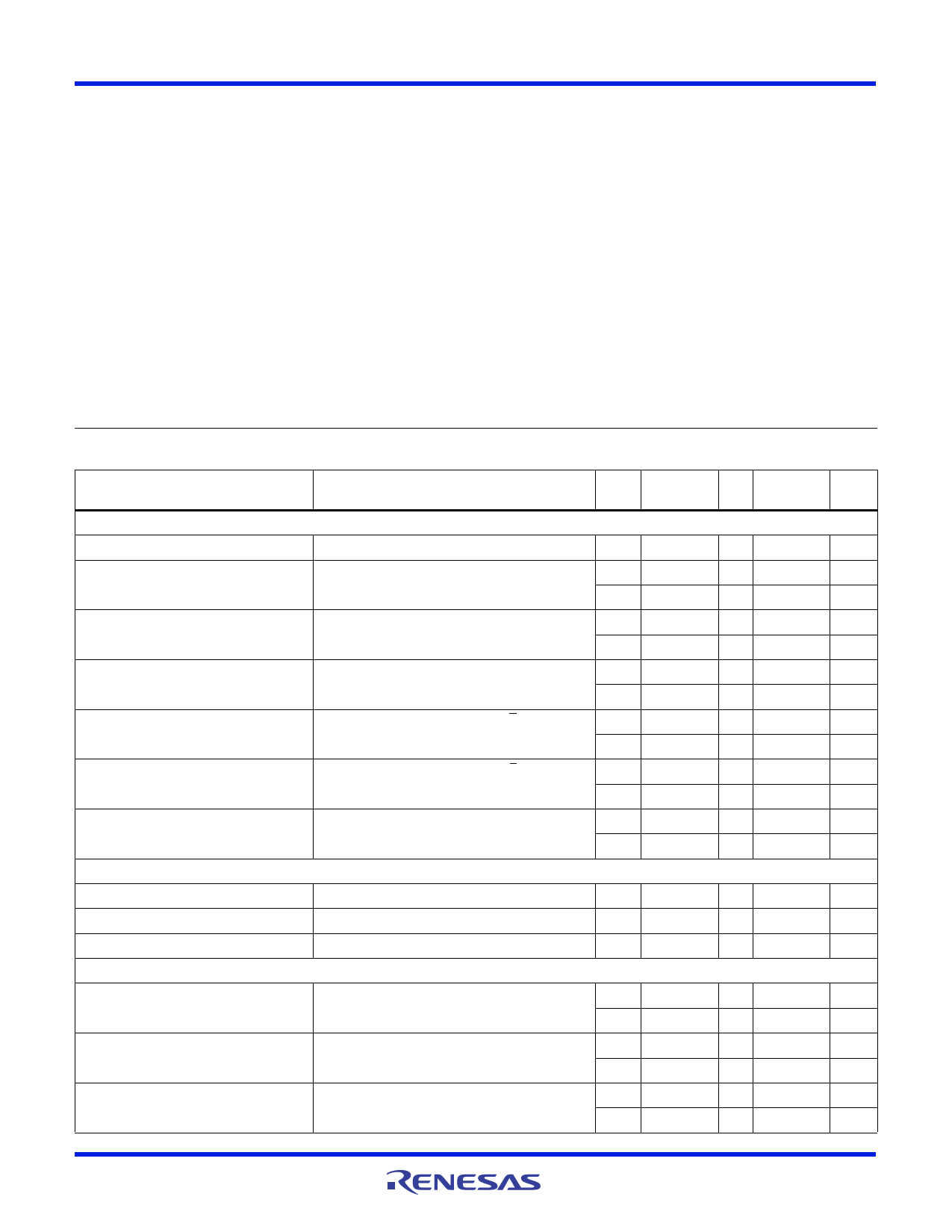
Electrical Specifications ±5V Supply Test Conditions: VSUPPLY = ±4.5V to ±5.5V, GND = 0V, VINH = 2.4V, VINL = 0.8V (Note 3),
Unless Otherwise Specified.
PARAMETER
TEST CONDITIONS
TEMP
MIN
MAX
(°C) (Notes 4, 8) TYP (Notes 4, 8) UNITS
ANALOG SWITCH CHARACTERISTICS
Analog Signal Range, VANALOG
ON-Resistance, rON
(Note 10)
VS = ±4.5V, ICOM = 2mA, VNO = 3V
(See Figure 5)
Full
V-
-
V+
V
25
-
44
60
Full
-
-
80
rON Matching Between Channels, rON VS = ±4.5V, ICOM = 2mA, VNO = 3V (Note 5)
25
-
1.3
4
Full
-
-
6
rON Flatness, rFLAT(ON)
VS = ±4.5V, ICOM = 2mA, VNO = ±3V, 0.1V
(Note 6)
25
-
7.5
9
Full
-
-
12
NO OFF Leakage Current, INO(OFF)
VS = ±5.5V, VCOM = 4.5V, VNO = +4.5V (Note 7) 25
-
0.02
-
nA
Full
-
0.2
-
nA
COM OFF Leakage Current, ICOM(OFF) VS = ±5.5V, VCOM = 4.5V, VNO = +4.5V (Note 7) 25
-
0.02
-
nA
Full
-
0.2
-
nA
COM ON Leakage Current, ICOM(ON)
VS = ±5.5V, VCOM = VNO = ±4.5V (Note 7)
25
-
0.02
-
nA
Full
-
0.2
-
nA
DIGITAL INPUT CHARACTERISTICS
Input Voltage High, VINHH, VADDH
Full
2.4
-
-
V
Input Voltage Low, VINHL, VADDL
Full
-
-
0.8
V
Input Current, IADDH, IADDL, IINHH, IINHL VS = ±5.5V, VINH, VADD = 0V or V+, (Note 9)
Full
-0.5
-
0.5
µA
DYNAMIC CHARACTERISTICS
INHIBIT Turn-ON Time, tON
VS = ±4.5V, VNO = ±3V, RL = 300, CL = 35pF,
25
-
35
50
ns
VIN = 0 to 3 (See Figure 1, Note 9)
Full
-
-
60
ns
INHIBIT Turn-OFF Time, tOFF
VS = ±4.5V, VNO = ±3V, RL = 300, CL = 35pF,
25
-
22
35
ns
VIN = 0 to 3 (See Figure 1, Note 9)
Full
-
-
40
ns
Address Transition Time, tTRANS
VS = ±4.5V, VNO = ±3V, RL = 300, CL = 35pF,
25
-
43
60
ns
VIN = 0 to 3 (See Figure 1, Note 9)
Full
-
-
70
ns
FN6416 Rev 3.00
April 13, 2009
Page 3 of 15
Share Link: 