CAT37 데이터 시트보기 (PDF) - ON Semiconductor
부품명
상세내역
일치하는 목록
CAT37 Datasheet PDF : 11 Pages
| |||
CAT37
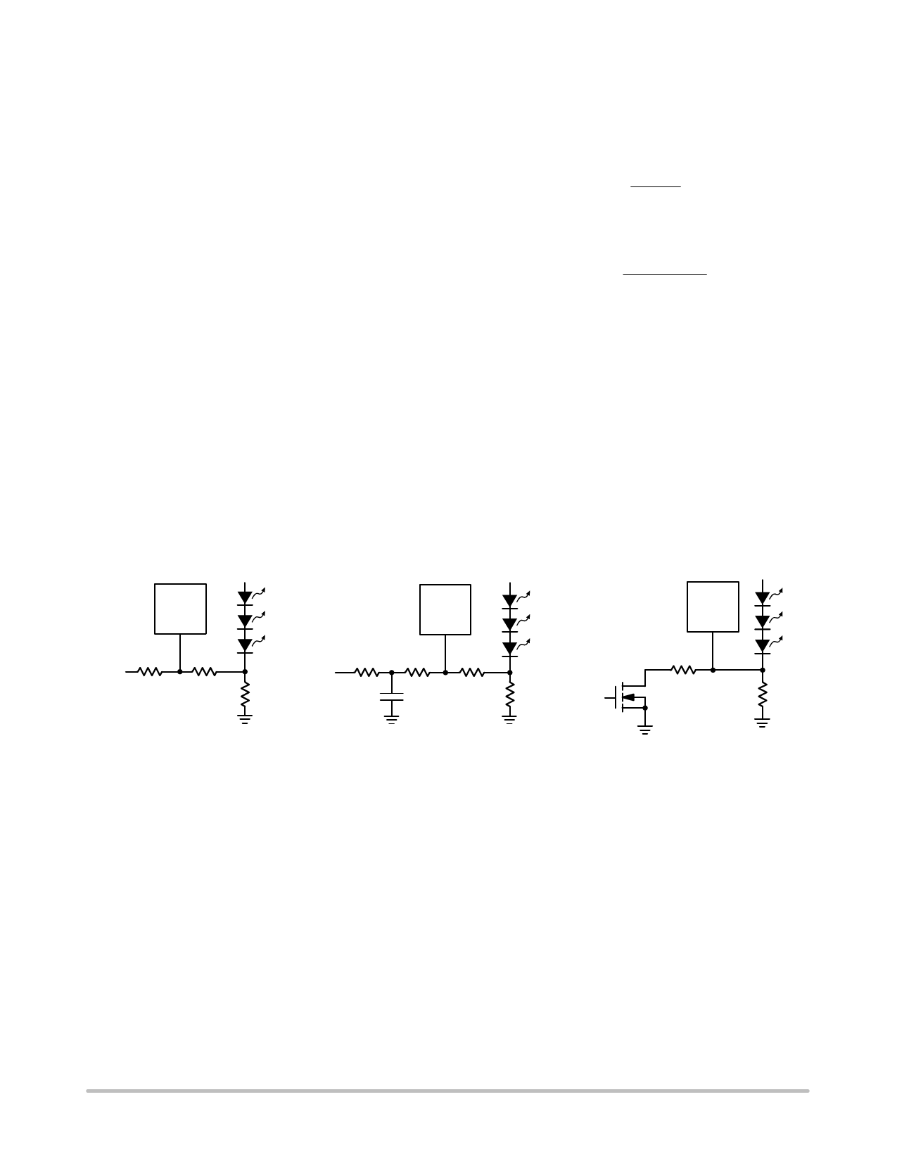
LED Dimming with DC Signal
Dimming the LEDs can be done by applying a variable
DC voltage as shown on Figure 14. As the VDC increase the
voltage across R1 decreases and therefore lower the LED
current. The resistors R2 and R3 must be large enough so
that their current (tens of mA) is much smaller than the LED
current but much larger than the FB leakage current (IFB).
When adjusting VDC between 0 V and 2 V, the resistors
shown on Figure 14 will set the LED current between 0 mA
and 15 mA.
LED Dimming with PWM Signal
PWM brightness control provides the widest dimming
range (greater than 20:1). By turning the LEDs ON and OFF
using the control signal, the LEDs operate at either zero or
full current, but their average current changes with the PWM
signal duty cycle. Typically, a 5 kHz to 40 kHz PWM signal
is used.
A filtered PWM signal is used to dim the LEDs, as shown
in Figure 15.
In addition to providing the widest dimming range, PWM
brightness control also ensures the “purest” white LED color
over the entire dimming range. The true color of a white
LED changes with operating current, and is the “purest”
white at a specific forward current, usually 15 mA or
20 mA. If the LED current is less than or more than this
value, the emitted light becomes more blue. Applications
involving color LCDs can find the blue tint objectionable.
LED Dimming with a Logic Signal
For applications that need to adjust the LED brightness in
discrete steps, a logic signal can be used as shown in
Figure 16. R1 sets the minimum LED current value (when
the NMOS switch is OFF):
R1
+
0.095 V
ILED(MIN)
RINCR determines how much LED current increases when
the external NMOS switch is turned ON.
0.095 V
RINCR + ILED(INCREASE)
PCB Layout Guidelines
The CAT37 is a high−frequency switching regulator
where proper PCB board layout and component placement
can minimize noise and radiation and increase efficiency. To
maximize efficiency, the CAT37 design has fast switch rise
and fall times. To prevent radiation and high frequency
resonance problems minimize the length and area of all
traces connected to the SW pin and use a ground plane under
the switching regulator.
The SW pin, schottky diode and capacitor C2 signal path
should be kept as short as possible. The ground connection
for the R1 resistor should be tied directly to the GND pin and
not be shared with other components.
CAT37
FB
R3
180 kW
VDC
R2
10 kW
R1
6.3 W
10 kW
PWM
CAT37
FB
R3
R2
180 kW 10 kW
0.1 mF
R1
Logic
6.3 W Signal
CAT37
FB
RINCR
2N7002
R1
6.3 W
Figure 14. Dimming with a
DC Voltage
Figure 15. Dimming with a
Filtered PWM Signal
Figure 16. Dimming with a
Logic Signal
http://onsemi.com
8
Share Link: 