IDT72V3622L10PFG 데이터 시트보기 (PDF) - Integrated Device Technology
부품명
상세내역
일치하는 목록
IDT72V3622L10PFG
Integrated Device Technology

IDT72V3622L10PFG Datasheet PDF : 29 Pages
| |||
IDT72V3622/72V3632/72V3642 CMOS 3.3V SyncBiFIFOTM
256 x 36 x 2, 512 x 36 x 2, 1,024 x 36 x 2
SIGNAL DESCRIPTION
RESET
After power up, a Master Reset operation must be performed by providing
a LOW pulse to RST1 and RST2 simultaneously. Afterwards, the FIFO
memories of the IDT72V3622/72V3632/72V3642 are reset separately by
taking their Reset (RST1, RST2) inputs LOW for at least four port-A Clock
(CLKA) and four port-B Clock (CLKB) LOW-to-HIGH transitions. The Reset
inputs can switch asynchronously to the clocks. A FIFO reset initializes the
internal read and write pointers and forces the Input Ready flag (IRA, IRB) LOW,
the Output Ready flag (ORA, ORB) LOW, the Almost-Empty flag (AEA, AEB)
LOW, and the Almost-Full flag (AFA, AFB) HIGH. Resetting a FIFO also forces
the Mailbox Flag (MBF1, MBF2) of the parallel mailbox register HIGH. After
a FIFO is reset, its Input Ready flag is set HIGH after two clock cycles to begin
normal operation.
A LOW-to-HIGH transition on a FIFO Reset (RST1, RST2) input latches
the value of the Flag Select (FS0, FS1) inputs for choosing the Almost-Full and
Almost-Empty offset programming method. (For details see Table 1, Flag
Programming, and the Programming the Almost-Empty and Almost-Full Flags
section). The relevant FIFO Reset timing diagram can be found in Figure 2.
FIRST WORD FALL THROUGH (FWFT)
After Master Reset, the FWFT select function is active, permitting a choice
between two possible timing modes: IDT Standard mode or First Word Fall
Through (FWFT) mode. Once the Reset (RST1, RST2) input is HIGH, a
HIGH on the FWFT input during the next LOW-to-HIGH transition of CLKA
(for FIFO1) and CLKB (for FIFO2) will select IDT Standard mode. This mode
uses the Empty Flag function (EFA, EFB) to indicate whether or not there
are any words present in the FIFO memory. It uses the Full Flag function (FFA,
FFB) to indicate whether or not the FIFO memory has any free space for
writing. In IDT Standard mode, every word read from the FIFO, including the
first, must be requested using a formal read operation.
Once the Reset (RST1, RST2) input is HIGH, a LOW on the FWFT input
during the next LOW-to-HIGH transition of CLKA (for FIFO1) and CLKB (for
FIFO2) will select FWFT mode. This mode uses the Output Ready function
(ORA, ORB) to indicate whether or not there is valid data at the data outputs
(A0-A35 or B0-B35). It also uses the Input Ready function (IRA, IRB) to indicate
whether or not the FIFO memory has any free space for writing. In the FWFT
mode, the first word written to an empty FIFO goes directly to data outputs, no
read request necessary. Subsequent words must be accessed by performing
a formal read operation.
COMMERCIAL TEMPERATURE RANGE
Following Reset, the level applied to the FWFT input to choose the desired
timing mode must remain static throughout FIFO operation. Refer to Figure 2
(Reset) for a First Word Fall Through select timing diagram.
ALMOST-EMPTY FLAG AND ALMOST-FULL FLAG OFFSET PROGRAM-
MING
Four registers in these devices are used to hold the offset values for the
Almost-Empty and Almost-Full flags. The port B Almost-Empty flag (AEB) Offset
register is labeled X1 and the port A Almost-Empty flag (AEA) Offset register
is labeled X2. The port A Almost-Full flag (AFA) Offset register is labeled Y1
and the port B Almost-Full flag (AFB) Offset register is labeled Y2. The index
of each register name corresponds to its FIFO number. The offset registers can
be loaded with preset values during the reset of a FIFO or they can be
programmed from port A (see Table 1).
FS0 and FS1 function the same way in both IDT Standard and FWFT
modes.
— PRESET VALUES
To load the FIFO's Almost-Empty flag and Almost-Full flag Offset registers
with one of the three preset values listed in Table 1, at least one of the flag select
inputs must be HIGH during the LOW-to-HIGH transition of its reset input. For
example, to load the preset value of 64 into X1 and Y1, FS0 and FS1 must be
HIGH when FlFO1 Reset (RST1) returns HIGH. Flag offset registers
associated with FIFO2 are loaded with one of the preset values in the same way
with FIFO2 Reset (RST2) toggled simultaneously with FIFO1 Reset (RST1).
For preset value loading timing diagram, see Figure 2.
— PARALLEL LOAD FROM PORT A
To program the X1, X2, Y1, and Y2 registers from port A, both FlFOs should
be reset simultaneously with FS0 and FS1 LOW during the LOW-to-HIGH
transition of the Reset inputs. After this reset is complete, the first four writes to
FIFO1 do not store data in the FIFO memory but load the offset registers in the
order Y1, X1, Y2, X2. The port A data inputs used by the offset registers are
(A7-A0), (A8-A0), or (A9-A0) for the IDT72V3622, IDT72V3632, or
IDT72V3642, respectively. The highest numbered input is used as the most
significant bit of the binary number in each case. Valid programming values for
the registers ranges from 1 to 252 for the IDT72V3622; 1 to 508 for the
IDT72V3632; and 1 to 1,020 for the IDT72V3642. After all the offset registers
are programmed from port A, the port B Full/Input Ready flag (FFB/IRB) is set
HIGH, and both FIFOs begin normal operation. See Figure 3 for relevant offset
register parallel programming timing diagram.
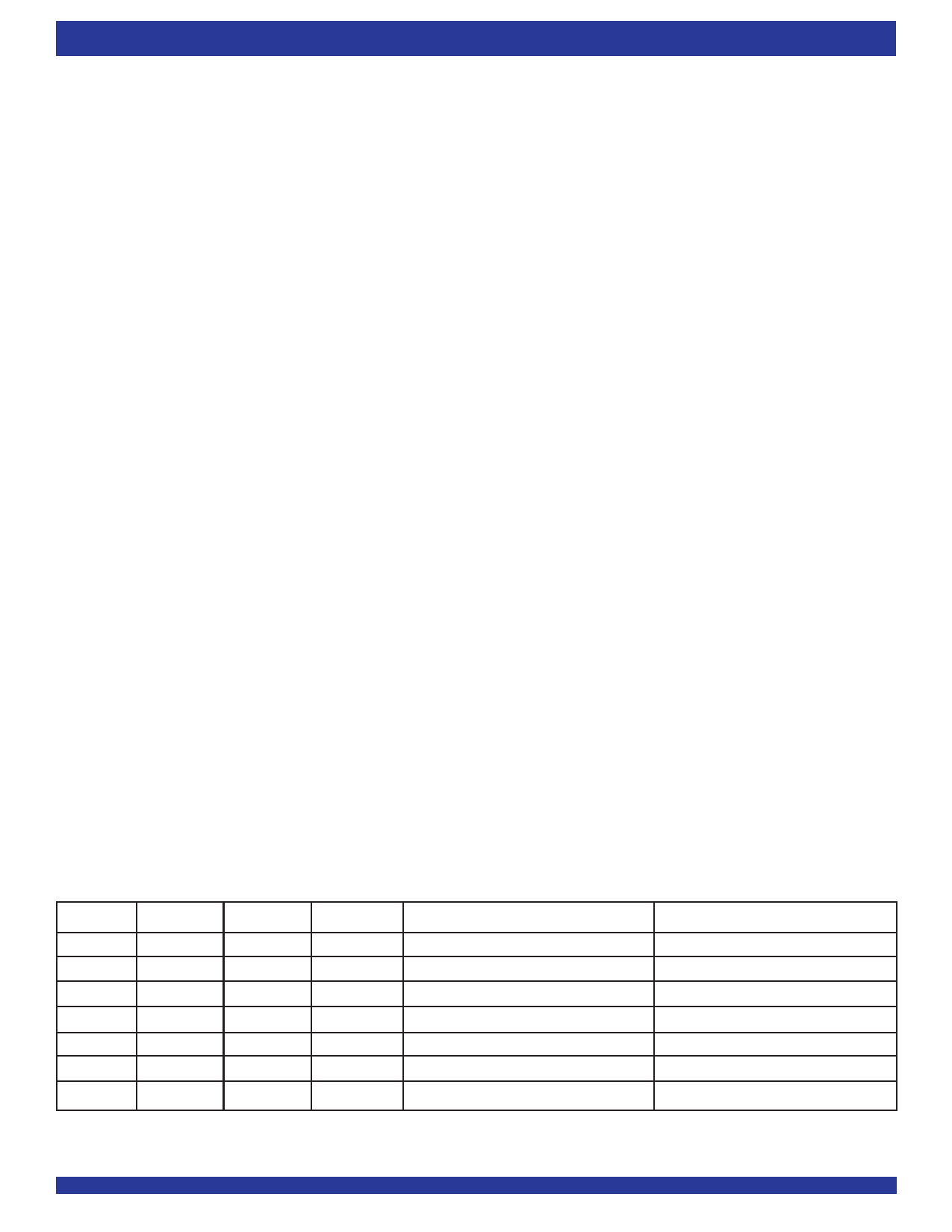
TABLE 1 — FLAG PROGRAMMING
FS1
FS0
RST1
RST2
H
H
↑
X
H
H
X
↑
H
L
↑
X
H
L
X
↑
L
H
↑
X
L
H
X
↑
L
L
↑
↑
NOTES:
1. X1 register holds the offset for AEB; Y1 register holds the offset for AFA.
2. X2 register holds the offset for AEA; Y2 register holds the offset for AFB.
X1 AND Y1 REGlSTERS(1)
64
X
16
X
8
X
Parallel programming via Port A
10
X2 AND Y2 REGlSTERS(2)
X
64
X
16
X
8
Parallel programming via Port A
Share Link: