AAT1156 데이터 시트보기 (PDF) - Advanced Analogic Technologies
부품명
상세내역
일치하는 목록
AAT1156 Datasheet PDF : 15 Pages
| |||
AAT1156
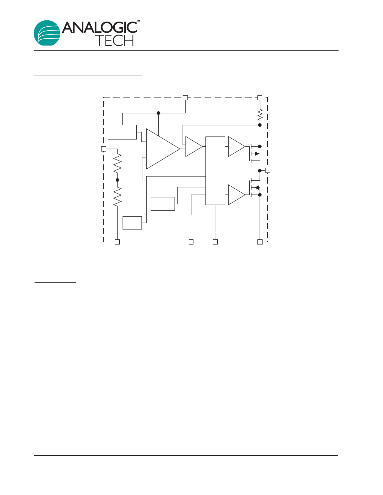
1MHz 700mA Step-Down DC-DC Converter
Functional Block Diagram
VCC
VP = 2.7V to 5.5V
1.0V REF
FB
OP. AMP
CMP
DH
LOGIC
LX
1MΩ
DL
Temp.
Sensing
OSC
SGND
EN
LL
PGND
Operation
Control Loop
The AAT1156 is a peak current mode step-down
converter. The inner wide bandwidth loop controls
the inductor peak current. The inductor current is
sensed through the P-channel MOSFET (high
side) and is also used for short-circuit and overload
protection. A fixed slope compensation signal is
added to the sensed current to maintain stability for
duty cycles greater than 50%. The loop appears
as a voltage-programmed current source in paral-
lel with the output capacitor.
The voltage error amplifier output programs the
current loop for the necessary inductor current to
force a constant output voltage for all load and line
conditions. The external voltage feedback resistive
divider divides the output voltage to the error ampli-
fier reference voltage of 0.6V. The voltage error
amplifier DC gain is limited. This eliminates the
need for external compensation components, while
still providing sufficient DC loop gain for good load
regulation. The voltage loop crossover frequency
and phase margin are set by the output capacitor.
Soft Start/Enable
Soft start increases the inductor current limit point in
discrete steps once the input voltage or enable
input is applied. It limits the current surge seen at
the input and eliminates output voltage overshoot.
When pulled low, the enable input forces the
AAT1156 into a non-switching shutdown state. The
total input current during shutdown is less than 1μA.
Power and Signal Source
Separate small signal ground and power supply
pins isolate the internal control circuitry from the
noise associated with the output MOSFET switch-
ing. The low pass filter R1 and C2 (shown in the
schematic in Figure 1) filters the input noise asso-
ciated with the power switching.
8
1156.2007.01.1.4
Share Link: 