74ALVC32PW 데이터 시트보기 (PDF) - NXP Semiconductors.
부품명
상세내역
일치하는 목록
74ALVC32PW Datasheet PDF : 13 Pages
| |||
NXP Semiconductors
74ALVC32
Quad 2-input OR gate
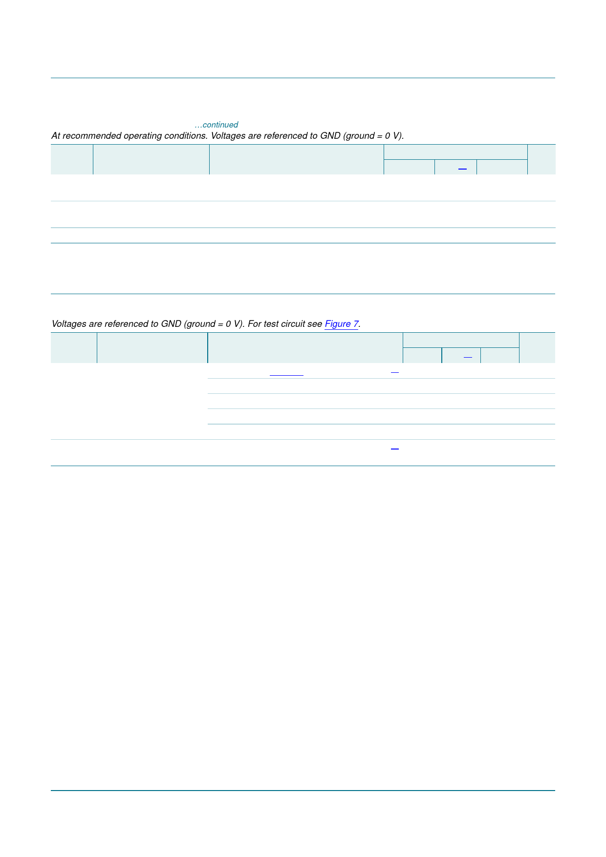
Table 6. Static characteristics …continued
At recommended operating conditions. Voltages are referenced to GND (ground = 0 V).
Symbol Parameter
Conditions
−40 °C to +85 °C
Min
Typ[1]
Max
ICC
∆ICC
CI
supply current
additional supply current
input capacitance
VCC = 3.6 V; VI = VCC or GND;
IO = 0 A
per input pin; VCC = 3.0 V to 3.6 V;
VI = VCC − 0.6 V; IO = 0 A
-
0.2
10
-
5
750
-
3.5
-
[1] All typical values are measured at VCC = 3.3 V (unless stated otherwise) and Tamb = 25 °C.
Unit
µA
µA
pF
10. Dynamic characteristics
Table 7. Dynamic characteristics
Voltages are referenced to GND (ground = 0 V). For test circuit see Figure 7.
Symbol Parameter
Conditions
tpd
propagation delay
CPD
power dissipation
capacitance
CP to Qn; see Figure 6
VCC = 1.65 V to 1.95 V
VCC = 2.3 V to 2.7 V
VCC = 2.7 V
VCC = 3.0 V to 3.6 V
per gate; VI = GND to VCC; VCC = 3.3 V
[1] Typical values are measured at Tamb = 25 °C
[2] tpd is the same as tPHL and tPLH.
[3] CPD is used to determine the dynamic power dissipation (PD in µW).
PD = CPD × VCC2 × fi × N + Σ(CL × VCC2 × fo) where:
fi = input frequency in MHz; fo = output frequency in MHz
CL = output load capacitance in pF
VCC = supply voltage in Volts
N = number of inputs switching
Σ(CL × VCC2 × fo) = sum of the outputs
−40 °C to +85 °C
Unit
Min Typ[1] Max
[2]
1.0
2.8
4.7 ns
1.0
2.0
3.1 ns
1.0
2.2
2.9 ns
1.0
2.0
2.8 ns
[3]
-
25
- pF
74ALVC32_2
Product data sheet
Rev. 02 — 10 December 2007
© NXP B.V. 2007. All rights reserved.
5 of 13
Share Link: 