SL22-L 데이터 시트보기 (PDF) - Willas Electronic Corp.
부품명
상세내역
일치하는 목록
SL22-L Datasheet PDF : 4 Pages
| |||
WILLAS
2.0A LOW VF SCHOTTKY BARRIER RECTIFIERS-20V-40V
1.0A SURFACE MOUNT SCHOTTKY BARRIESRMSRAOE-DCL-TS1I2FP3IE+ARCSPK-A2AC0GVKE-A2G0E0V
FM120-M+
SL22-LTHRU
SLF24M-1L200-M+
Pb Free Product
PacFkienagtuinrefosrmation
• Batch process design, excellent power dissipation offers
better reverse leakage current and thermal resistance.
• Low profile surface mounted application in order to
optimize board space.
P0
• Low power loss, high efficiency.
• High current capability, low forward voltage droPp1.
• High surge capability.
d
• Guardring for overvoltage protection.
•EUltra high-speed switching.
• Silicon epitaxial planar chip, metal silicon junction.
F
• Lead-free parts meet environmental standards of
MIL-STD-19500 /228
B
• RoHS product for packing code suffix "G"
Halogen free product for packing code suffix "H"
Mechanical data
• Epoxy : ULA94-V0 rated flame retardant P
• Case : Molded plastic, SOD-123H
,
• Terminals :Plated terminals, solderable per MIL-STD-750
Method 2026
• Polarity : Indicated by cathode band
• Mounting Position : Any
• Weight : Approximated 0.011 gram
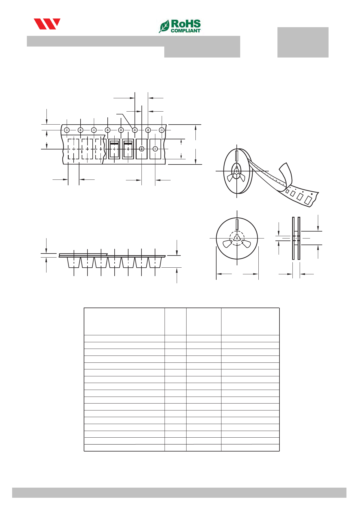
Package outline
SOD-123H
0.146(3.7)
0.130(3.3)
0.012(0.3) Typ.
0.071(1.8)
0.056(1.4)
W
0.031(0.8) Typ.
0.040(1.0)
0.024(0.6)
0.031(0.8) Typ.
Dimensions in inches and (millimeters)
MAXIMUM RATINGS AND ELECTRICAL CHARACTERISTICS
D2
D1
RatingTs at 25℃ ambient temperature unless otherwise specified.
Single phase half wave, 60Hz, resistive of inductive load.
C
For capacitive load, derate current by 20%
RATINGS
W1
SYMBOL FM120-MH FM130-MH FM140-MH FM150-MDH FM160-MH FM180-MH FM1100-MH FM1150-MH FM1200-MH UN
Marking Code
12
13
14
15
16
18
10
115 120
Maximum Recurrent Peak Reverse Voltage
VRRM
20
30
40
50
60
80
100
150
200 Volt
Maximum RMS Voltage
VRMS
14
21
28
35
42
56
70
105
140 Volt
Maximum DC Blocking Voltage
VDC
20
30
40
50
60 unit:mm80
100
150
200 Volt
Maximum Average Forward Rectified Current
IO
1.0
Amp
Item
Peak Forward Surge Current 8.3 ms single half sine-wave
superimposed on rated load (JEDEC method)
IFSM
Symbol Tolerance
SMA-LS
30
Amp
Typical Thermal Resistance (Note C2)arrier width
RΘJA
Typical Junction Capacitance (NoteC1a)rrier length
CJ
Operating Temperature Range Carrier depth
TJ
Storage Temperature Range
Sprocket hole
TSTG
13" Reel outside diameter
A
0.1
B
0.1
C -55 to +1250.1
d
0.1
D
2.0
2.8400
5.01020
1.90
- 16.550to +175
330.00
-55 to +150
℃/W
PF
℃
℃
CHARACTERI1S3T"ICRSeel
inner diameter
SYMBOL
D1
min
50.00
FM120-MH FM130-MH FM140-MH FM150-MH FM160-MH FM180-MH FM1100-MH FM1150-MH FM1200-MH
UNI
Maximum Forward Voltage at 1.0A7D"CReel outside diametVeFr
D
0.520.0
0.70178.00
0.85
0.9
0.92 Volt
7" Reel inner diameter
D1
min
62.00
Maximum Average Reverse Current at @T A=25℃
Feed hole diameter
IR
D2
0.5
0.5
13.00
mAm
Rated DC Blocking Voltage
Sproc@keTt Ah=o1le25p℃osition
E
0.1
1.7150
NOTES:
Punch hole position
1- Measured at 1 MHZ and applied rePveurnsechvohltoalgeepoiftc4h.0 VDC.
Sprocket hole pitch
2- Thermal Resistance From Junction to Ambient
Embossment center
F
0.1
P
0.1
P0
0.1
P1
0.1
5.50
4.00
4.00
2.00
Overall tape thickness
T
0.1
0.23
Tape width
W
0.3
12.00
Reel width
W1
1.0
18.00
Note:Devices are packed in accor dance with EIA standar RS-481-A and specifications listed above.
2012-06
201-
WILLAS ELECTRONIC CORP.
WILLAS ELECTRONIC CORP.
Share Link: 