CS8164 데이터 시트보기 (PDF) - ON Semiconductor
부품명
상세내역
일치하는 목록
CS8164 Datasheet PDF : 8 Pages
| |||
Definition of Terms
Dropout Voltage
The input-output voltage differential at which the circuit
ceases to regulate against further reduction in input volt-
age. Measured when the output voltage has dropped
100mV from the nominal value obtained at 14V input,
dropout voltage is dependent upon load current and junc-
tion temperature.
Input Voltage
The DC voltage applied to the input terminals with respect
to ground.
Input Output Differential
The voltage difference between the unregulated input
voltage and the regulated output voltage for which the
regulator will operate.
Line Regulation
The change in output voltage for a change in the input
voltage. The measurement is made under conditions of
low dissipation or by using pulse techniques such that the
average chip temperature is not significantly affected.
Load Regulation
The change in output voltage for a change in load current
at constant chip temperature.
Long Term Stability
Output voltage stability under accelerated life-test condi-
tions after 1000 hours with maximum rated voltage and
junction temperature.
Output Noise Voltage
The rms AC voltage at the output, with constant load and
no input ripple, measured over a specified frequency
range.
Quiescent Current
The part of the positive input current that does not con-
tribute to the positive load current. i.e., the regulator
ground lead current.
Ripple Rejection
The ratio of the peak-to-peak input ripple voltage to the
peak-to-peak output ripple voltage.
Temperature Stability of VOUT
The percentage change in output voltage for a thermal
variation from room temperature to either temperature
extreme.
Current Limit
Peak current that can be delivered to the output.
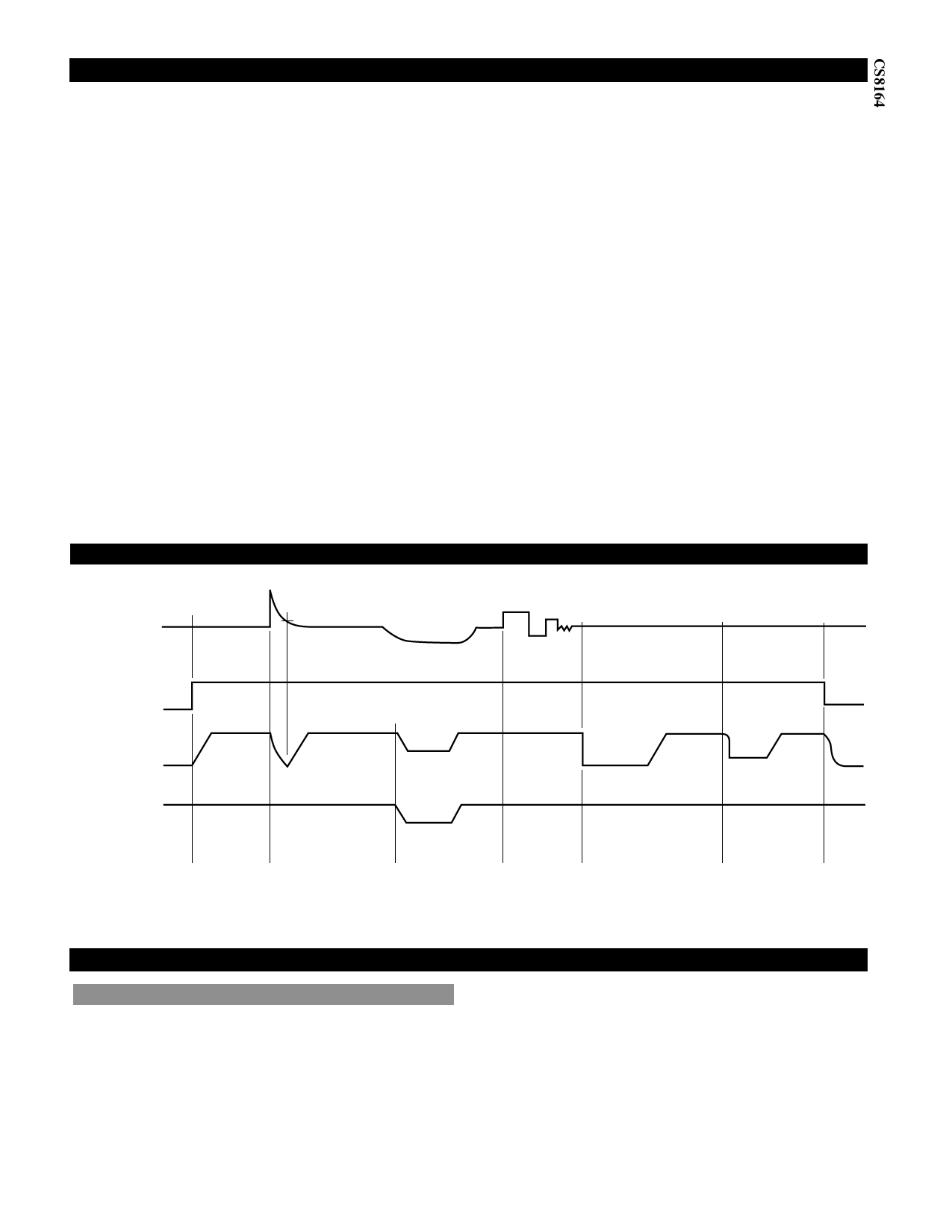
Typical Circuit Waveform
60V
VIN 14V
31V
26V
3V
14V
ENABLE 2.0V
0.8V
VOUT1 0V
VOUT2 5V
8V
8V
8V
8V
2.4V
0V
5V
5V
2.4V
8V
0V
System
Condition
Turn
On
Load
Dump
Low VIN
Line Noise, Etc.
VOUT2
Short
Circuit
Thermal
Shutdown
Turn
Off
Circuit Description
Standby Output
The CS8164 is equipped with two outputs. The second
output is intended for use in systems requiring standby
memory circuits. While the high current primary output
can be controlled with the ENABLE lead described below,
the standby output remains on under all conditions as long
as sufficient input voltage is applied to the IC. Thus, mem-
ory and other circuits powered by this output remain unaf-
fected by positive line transients, thermal shutdown, etc.
The standby regulator circuit is designed so that the quies-
cent current to the IC is very low (<2mA) when the other
regulator output is off.
In applications where the standby output is not needed, it
may be disabled by connecting a resistor from the standby
output to the supply voltage. This eliminates the need for
a capacitor on the output to prevent unwanted oscilla-
tions. The value of the resistor depends upon the mini-
mum input voltage expected for a given system. Since the
standby output is shunted with an internal 6.0V Zener, the
current through the external resistor should be sufficient
5
Share Link: 