SNAD02C 데이터 시트보기 (PDF) - Sonix Technology Co., Ltd
부품명
상세내역
일치하는 목록
SNAD02C Datasheet PDF : 27 Pages
| |||
SNAD02C
8-CHANNEL 10-BIT ADC
(1) The power down command (000/111) is sent to SNAD02C in the first three cycles, and then
SNAD02C enters into power down mode at the 8th clock cycle, consuming almost no current
(less than 1uA).
(2) After SNAD02C enters power down (mode 0: command 000), SNAD02C sends “0” out to
DIO until a valid logic transition appears on any wakeup-enabled digital input channel. Once
the transition occurs, SNAD02C toggles DIO to “1” to inform host controller. After receiving
“1” from DIO, host controller should turn START back to “1” to inform SNAD02C that the
power-down stage is over. Otherwise, SNAD02C keeps sending out “1” to DIO and does not
recognize any other transitions on any channels.
(3) After SNAD02C enters power down (mode 1: command 111), SNAD02C sends “1” out to
DIO until a valid logic transition appears on any wakeup-enabled digital input channel. Once
the transition occurs, SNAD02C toggles DIO to “0” to inform host controller. After receiving
“0” from DIO, host controller should turn START back to “1” to inform SNAD02C that the
power-down stage is over. Otherwise, SNAD02C keeps sending out “1” to DIO and does not
recognize any other transitions any the channels.
(4) The CLK may stop but START ought to remain at LOW level in the whole power down mode.
(5) The SNAD02C provides two power-down mode “POWER_DOWN 0” and
“POWER_DOWN 1”, user has to select a property power-down mode that it depend
on what kind I/O type for host MCU (pull-up or pull-low) before ADC enter
power-down mode. Otherwise, it will generate a DC-path and the standby current
also will go up.
(6) Before into power down mode, the “RF” and “MB” register must set up “0”, otherwise
the standby current will more than 1uA.
Note:
Wakeup function is only dedicated to the channel which is digital input type AND wakeup-enabled.
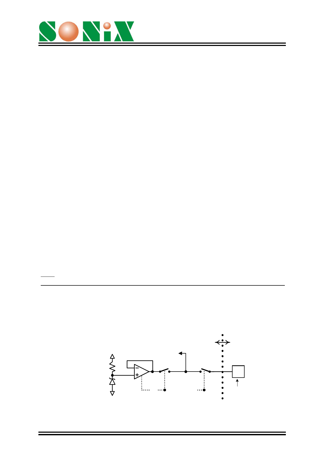
6.7. Bandgap reference
VDD
1.2v
bandgap
reference
VSS
to reference
high of the ADC
ON CHIP
RF
MB
OFF CHIP
REF
PAD
Figure-10 Circuit diagram of ADC bandgap reference selection
Version: 1.3
11
July 31, 2003
Share Link: 