MB88151A 데이터 시트보기 (PDF) - Cypress Semiconductor
부품명
상세내역
일치하는 목록
MB88151A Datasheet PDF : 27 Pages
| |||
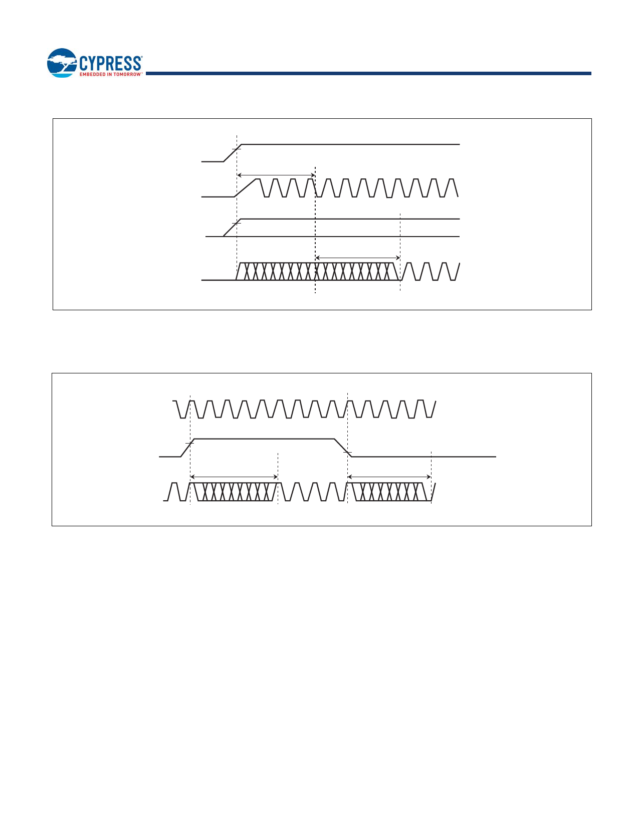
16. Lock-up Time
VDD
3.0 V
Internal clock
stabilization wait time
XIN
Setting pin
SEL0,
VIH
SEL1,
ENS
CKOUT
tLK
(lock-up time )
MB88151A
If the setting pin is fixed at the “H” or “L” level, the maximum time after the power is turned on until the set clock signal is output from
CKOUT pin is (the stabilization wait time of input clock to XIN pin) + (the lock-up time “tLK”). For the input clock stabilization time,
check the characteristics of the resonator or oscillator used.
XIN
VIH
ENS
CKOUT
tLK
(lock-up time )
VIL
tLK
(lock-up time )
For modulation enable control using the ENS pin during normal operation, the set clock signal is output from
CKOUT pin at most the lock-up time (tLK) after the level at the ENS pin is determined.
Note : When the pin setting is changed, the CKOUT pin output clock stabilization time is required. Until the output clock signal becomes
stable, the output frequency, output clock duty cycle, modulation period, and cycle-cycle jitter cannot be guaranteed. It is
therefore advisable to perform processing such as cancelling a reset of the device at the succeeding stage after the lock-up time.
Document Number: 002-08311 Rev. *B
Page 18 of 26
Share Link: 