MC33989(2002) 데이터 시트보기 (PDF) - Freescale Semiconductor
부품명
상세내역
일치하는 목록
MC33989 Datasheet PDF : 32 Pages
| |||
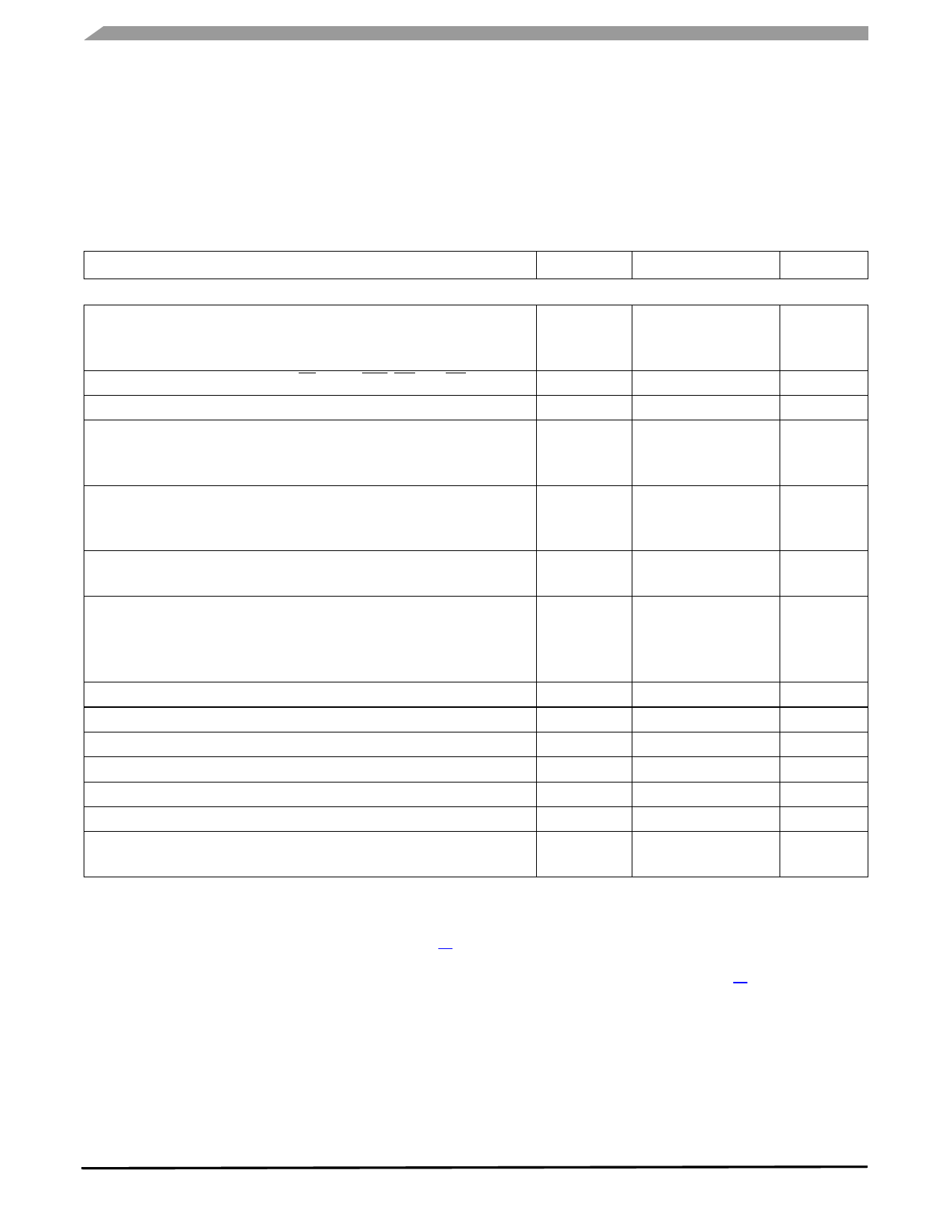
MC33989
Freescale Semiconductor, Inc.
(Vsup From 5.5V to 18V and Tamb -40°C to 125°C)
For all pins except CANH, CANL, Tx and Rx which are described in the CAN module section
Description
Dropout Voltage
Dropout Voltage, limited output current
Symbol
Vdd1drop
Vdd1dp2
Characteristics
Min
Typ
Max
0.2
0.5
0.1
0.25
Unit
V
V
Idd1 output current
Idd1
200
285
350
mA
Thermal Shutdown (junction)
Tsd
160
200
°C
Over temperature pre warning (junction)
Tpw
125
160
°C
Temperature Threshold difference
Tsd-Tpw
20
40
°C
Reset threshold 1
Rst-th1
4.5
4.6
4.7
V
Reset threshold 2
Vdd1 range for Reset Active
Rst-th2
4.1
4.2
4.3
V
Vddr
1
V
Reset Delay Time
td
4
30
us
Line Regulation (C at Vdd1= 47uF tantal)
Line Regulation (C at Vdd1= 47uF tantal)
Load Regulation (C at Vdd1= 47uF tantal)
LR1
LR2
LD
5
25
mV
10
25
mV
25
75
mV
Thermal stability
ThermS
30
50
mV
Vdd1 in Stop mode
Vdd1 Output Voltage
Vdd1 Output Voltage
Idd1 stop output current to wake up SBC
Idd1 over current wake up deglitcher time
Reset threshold
Reset threshold
Line regulation (C at Vdd1= 47uF tantal)
Load regulation (C at Vdd1= 47uF tantal)
Vddstop
Vddstop2
Idd1s-wu
Idd1 - dglt
Rst-stop1
Rst-stop2
LR-s
LD-s
4.75
4.75
10
40
4.5
4.1
5,00
5,00
17
55
4.6
4.2
5
15
5.25
V
5.25
V
25
mA
75
us
4.7
V
4.3
V
25
mV
75
mV
Conditions
Idd1 = 200mA
Idd1 = 50mA
4.5V< Vsup
Internally limited
Normal or standby mode
VDDTEMP bit set
Selectable by SPI. Default
value after reset.
Selectable by SPI
Measured at 50% of reset
signal
9V<Vsup<18, Idd=10mA
5.5V<Vsup<27V, Idd=10mA
1mA<IIdd<200mA
Vsup=13.5V, I=100mA
not tested, guaranted by
charaterization and design
Idd1<=2mA
Idd1<=10mA
guaranted by design
5.5V<Vsup<27V, Idd=2mA
1mA<IIdd<10mA
V2 tracking voltage regulator
note 3: V2 specification with external capacitor
- Stability requirement: C>42uF and ESR<1.3 ohm (tantalum capacitor), external resistor between base and emitter required.
- Measurement conditions: Ballast transistor MJD32C, C=10uF tantalum, 2.2k resistor between base and emitter of ballast transistor.
V2 Output Voltage (C at V2 = 10uF tantal)
V2
0.99
1
1.01
Vdd1
I2 from 2 to 200mA
5.5V< Vsup <27V
I2 output current (for information only)
I2
200
mA
Depending upon external
ballast transistor
V2 ctrl drive current capability
I2ctrl
0
10
mA
Worst case at Tj=125°C
V2LOW Flag Threshold
V2Lth
3.75
4
4.25
V
Logic output pins (MISO) Push pull structure with tri state condition (CSB high).
Low Level Output Voltage
Vol
0
1.0
V
I out = 1.5mA
High Level Output Voltage
Voh
Vdd1-0.9
Vdd1
V
I out = -250uA
Tristated MISO Leakage Current
-2
Logic input pins (MOSI, SCLK, CSB)
+2
uA
0V<Vmiso<Vdd
High Level Input Voltage
Vih
0.7Vdd1
Vdd1+0.3
Low Level Input Voltage
Vil
-0.3
0.3Vdd1
V
High Level Input Current on CSB
Low Level Input Current CSB
MOSI, SCK Input Current
Iih
-100
Iil
-100
Iin
-10
-20
uA
-20
uA
10
uA
Vi=4V
Vi=1V
0<VIN<Vdd
MC33989
For More Information On This Product,
4
Go to: www.freescale.com
Share Link: 