NCP305 데이터 시트보기 (PDF) - ON Semiconductor
부품명
상세내역
일치하는 목록
NCP305 Datasheet PDF : 23 Pages
| |||
NCP304, NCP305
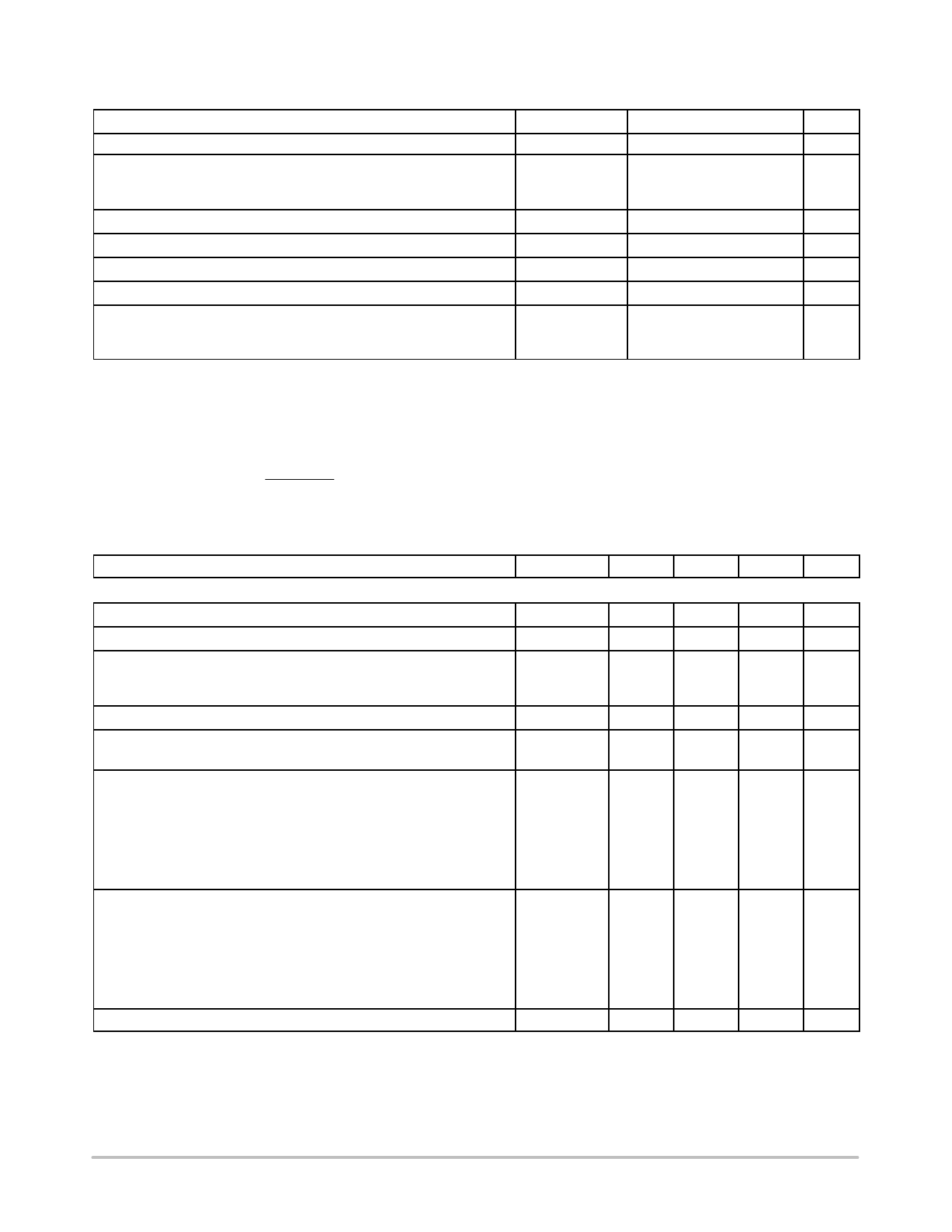
MAXIMUM RATINGS (Note 1)
Rating
Symbol
Value
Unit
Input Power Supply Voltage (Pin 2)
Output Voltage (Pin 1)
Complementary, NCP304
N−Channel Open Drain, NCP305
Vin
VOUT
12
V
V
−0.3 to Vin+0.3
−0.3 to 12
Output Current (Pin 1) (Note 2)
Thermal Resistance, Junction−to−Air
Maximum Junction Temperature
Storage Temperature Range
Latchup Performance (Note 3)
Positive
Negative
IOUT
RqJA
TJ
Tstg
ILATCHUP
70
285
+125
−55 to +150
500
170
mA
°C/W
°C
°C
mA
Stresses exceeding Maximum Ratings may damage the device. Maximum Ratings are stress ratings only. Functional operation above the
Recommended Operating Conditions is not implied. Extended exposure to stresses above the Recommended Operating Conditions may affect
device reliability.
1. This device series contains ESD protection and exceeds the following tests:
Human Body Model 2000 V per MIL−STD−883, Method 3015.
Machine Model Method 200 V.
2. The maximum package power dissipation limit must not be exceeded.
PD
+
TJ(max)−TA
RqJA
3. Maximum Ratings per JEDEC standard JESD78.
ELECTRICAL CHARACTERISTICS (For all values TA = 25°C, unless otherwise noted.)
Characteristic
Symbol
Min
Typ
Max
Unit
NCP304/5 − 0.9
Detector Threshold (Pin 2, Vin Decreasing)
Detector Threshold Hysteresis (Pin 2, Vin Increasing)
Supply Current (Pin 2)
(Vin = 0.8 V)
(Vin = 2.9 V)
Maximum Operating Voltage (Pin 2)
Minimum Operating Voltage (Pin 2)
(TA = −40°C to 85°C)
Reset Output Current (Pin 1, Active Low ‘L’ Suffix Devices)
N−Channel Sink Current, NCP304, NCP305
(VOUT = 0.05 V, Vin = 0.70 V)
(VOUT = 0.50 V, Vin = 0.85 V)
P−Channel Source Current, NCP304
(VOUT = 2.4 V, Vin = 4.5 V)
VDET−
VHYS
Iin
Vin(max)
Vin(min)
IOUT
0.882
0.900
0.918
V
0.027
0.045
0.063
V
mA
−
0.8
2.4
−
−
3.0
−
−
10
V
−
0.55
0.70
V
−
0.65
0.80
mA
0.01
0.05
−
0.05
0.50
−
1.0
2.0
−
Reset Output Current (Pin 1, Active High ‘H’ Suffix Devices)
N−Channel Sink Current, NCP304, NCP305
(VOUT = 0.5 V, Vin = 1.5 V)
IOUT
1.05
2.5
mA
−
P−Channel Source Current, NCP304
(VOUT = 0.4 V, Vin = 0.7 V)
(VOUT = GND, Vin = 0.8 V)
Propagation Delay Input to Output (Figure 2)
0.011
0.04
−
0.014
0.08
−
ms
4. In the case of CMOS Output Type: The time interval between the rising edge of VDD input pulse from 0.7 V to (+VDET) +2.0 V and output
voltage level becoming to VDD/2. In the case of N−Channel Open Drain Output Type: Output pin is pulled up with a resistance of 470 kW
to 5.0 V, the time interval between the rising edge of VDD input pulse from 0.7 V to (+VDET) +2.0 V and output voltage level becoming to
2.5 V.
http://onsemi.com
2
Share Link: 