NCP565 데이터 시트보기 (PDF) - ON Semiconductor
부품명
상세내역
일치하는 목록
NCP565 Datasheet PDF : 15 Pages
| |||
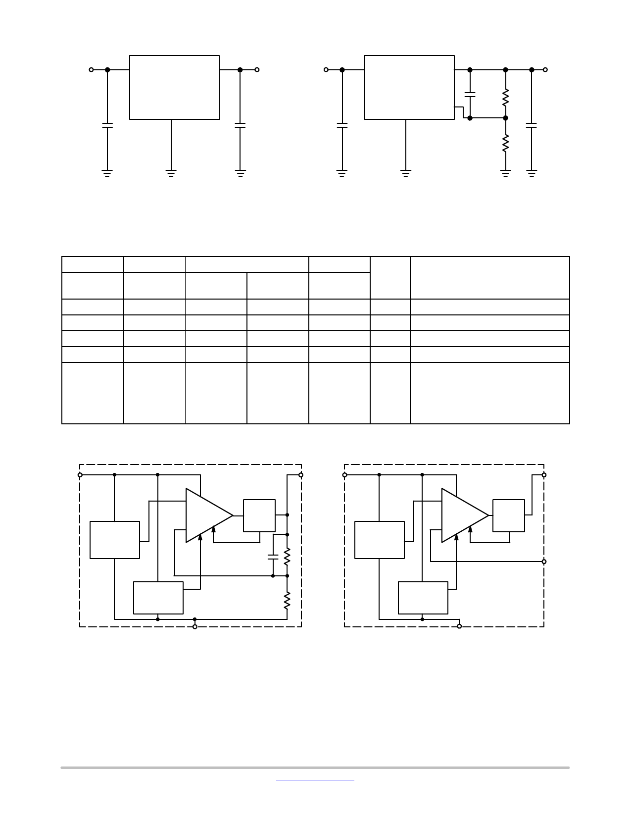
Vin
Cin
Vin
Vout
NCP565
GND
NCP565, NCV565
Vout
Vin
Cout
Cin
Vin
Vout
NCP565
GND ADJ
C1
R1
5.6 pF
R2
Vout
Cout
Figure 1. Typical Application Schematic,
Fixed Output
Figure 2. Typical Application Schematic,
Adjustable Output
PIN DESCRIPTION
D2PAK 5
D2PAK 3
Pin No.
Pin No.
Adj. Version Fixed Version
1
−
2
1
3, Tab
2, Tab
4
3
5
−
DFN6
SOT−223
Pin No.
Pin No.
Pin No.
Adj. Version Fixed Version Fixed Version Symbol
1, 2
1, 2, 5
−
N.C.
3
3
3
Vin
6
6
1
Ground
4
4
2, Tab
Vout
5
−
−
Adj
Description
−
Positive Power Supply Input Voltage
Power Supply Ground
Regulated Output Voltage
This pin is to be connected to the sense
resistors on the output. The linear
regulator will attempt to maintain 0.9 V
between this pin and ground. Refer to
the Application Information section for
output voltage setting.
Vin
Vref = 0.9 V
Voltage
Reference
Block
Output
Stage
Thermal
Shutdown
Block
GND
Current
Limit
Sense
Vout Vin
Vref = 0.9 V
Voltage
Reference
Block
Output
Stage
Current
Limit
Sense
Thermal
Shutdown
Block
GND
Vout
ADJ
Figure 3. Block Diagram, Fixed Output
Figure 4. Block Diagram, Adjustable Output
www.onsemi.com
2
Share Link: 