74F374 데이터 시트보기 (PDF) - Fairchild Semiconductor
부품명
상세내역
일치하는 목록
74F374 Datasheet PDF : 7 Pages
| |||
Unit Loading/Fan Out
Pin Names
D0–D7
CP
OE
O0–O7
Description
Data Inputs
Clock Pulse Input (Active Rising Edge)
3-STATE Output Enable Input (Active LOW)
3-STATE Outputs
U.L.
Input IIH/IIL
HIGH/LOW
Output IOH/IOL
1.0/1.0
20 µA/−0.6 mA
1.0/1.0
20 µA/−0.6 mA
1.0/1.0
20 µA/−0.6 mA
150/40 (33.3) −3 mA/24 mA (20 mA)
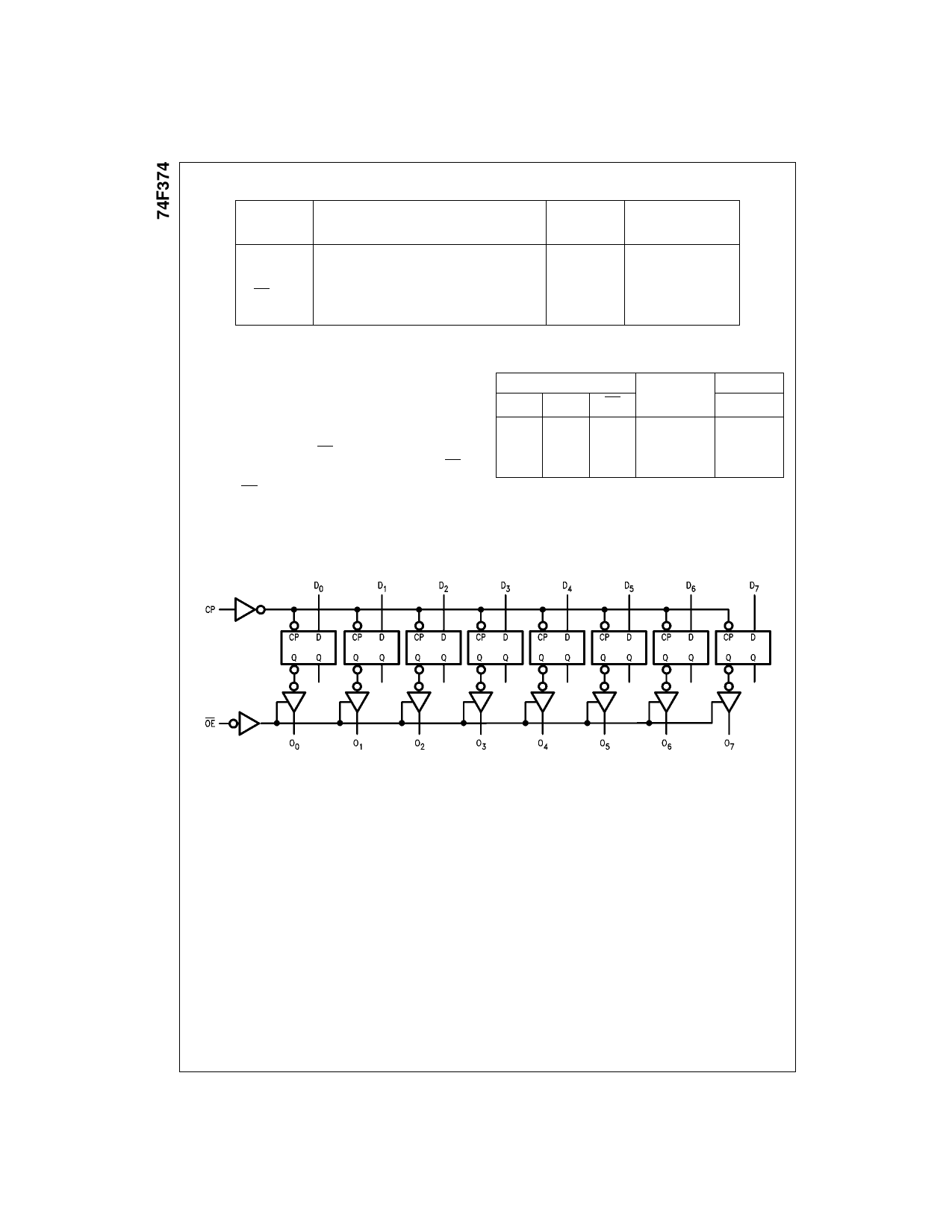
Functional Description
The 74F374 consists of eight edge-triggered flip-flops with
individual D-type inputs and 3-STATE true outputs. The
buffered clock and buffered Output Enable are common to
all flip-flops. The eight flip-flops will store the state of their
individual D inputs that meet the setup and hold time
requirements on the LOW-to-HIGH Clock (CP) transition.
With the Output Enable (OE) LOW, the contents of the
eight flip-flops are available at the outputs. When the OE is
HIGH, the outputs go to the high impedance state. Opera-
tion of the OE input does not affected the state of the flip-
flops.
Truth Table
Inputs
Dn
H
CP
OE
L
L
L
X
X
H
H = HIGH Voltage Level
L = LOW Voltage Level
X = Immaterial
Z = High Impedance
= LOW-to-HIGH Clock Transition
Internal
Register
H
L
X
Output
On
H
L
Z
Logic Diagram
Please note that this diagram is provided only for the understanding of logic operations and should not be used to estimate propagation delays.
www.fairchildsemi.com
2
Share Link: 