TDA1170N 데이터 시트보기 (PDF) - STMicroelectronics
부품명
상세내역
일치하는 목록
TDA1170N Datasheet PDF : 8 Pages
| |||
TDA1170N
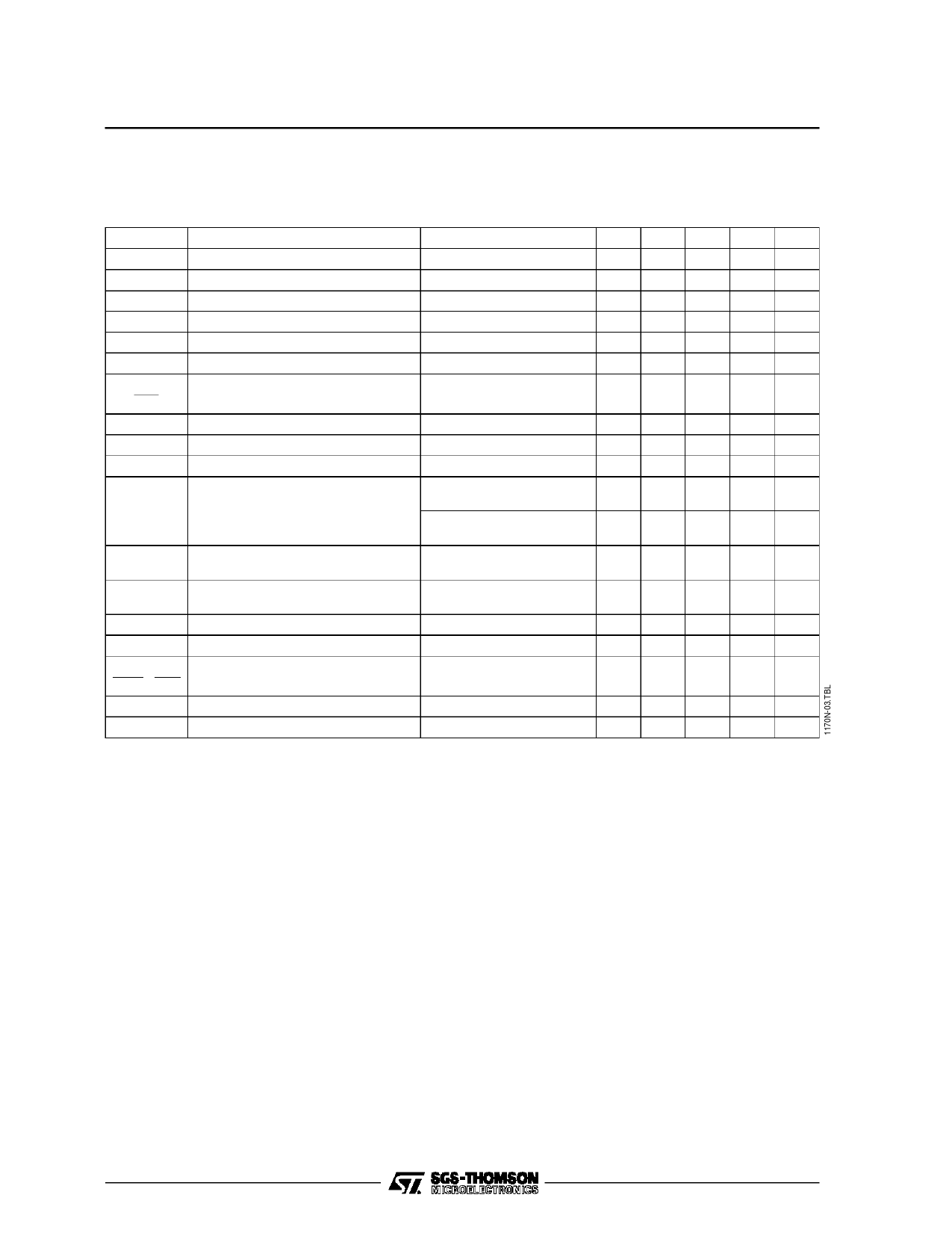
ELECTRICAL CHARACTERISTICS
(Refer to the test circuits, VS = 35 V, Tamb = 25oC,unless otherwise specified)
DC CHARACTERISTICS
Symbol
Parameter
Test Conditions
Min. Typ. Max. Unit Fig.
I2
Pin 2 Quiescent Current
I3 = 0
7 14 mA 1b
I5
Pin 5 Quiescent Current
I4 = 0
8 17 mA 1b
– I9
Oscillator Bias Current
V9 = 1V
0.1 1 µA 1a
– I10
Amplifier Input Bias Current
V10 = 1V
1
10 µA 1b
– I12
Ramp Generator Bias Current
V12 = 0
0.02 0.3 µA 1a
– I12
Ramp Generator Current
I7 = 20µA, V12 = 0
18.5 20 21.5 µA 1b
∆I12
I12
Ramp Generator Non-linearity
∆V12 = 0 to 12V, I7 = 20µA
0.2 1
% 1b
Vs
Supply Voltage Range
10
35 V
V1
Pin 1 Saturation Voltage to Ground I1 = 1mA
1 1.4 V
V3
Pin 3 Saturation Voltage to Ground I3 = 10mA
300 450 mV 1a
V4
Qiuescent output Voltage
VS = 10V
R1 = 1kΩ, R2 = 1kΩ
4.1 4.4 4.75 V 1a
VS = 35V
R1 = 3kΩ, R2 = 1kΩ
8.3 8.8 9.45 V 1a
V4L
Output Saturation Voltage to Ground – I4 = 0.1A
– I4 = 0.8A
0.9 1.2 V 1c
1.9 2.3 V 1c
V4H
Output Saturation Voltage to Supply I4 = 0.1A
I4 = 0.8A
1.4 2.1 V 1d
2.8 3.2 V 1d
V6
Regulated Voltage at Pin 6
6.1 6.5 6.9 V 1b
V7
Regulated Voltage at Pin 7
I7 = 20µA
6.2 6.6 7
V 1b
|∆V6|
∆VS
;
∆V7
∆VS
Regulated Voltage Drift with Supply
Voltage
∆VS = 10 to 35V
1
mV/V 1b
V10
Amplifier Input Reference Voltage
2.07 2.2 2.3 V
R8
Pin 8 Input Resistance
V8 ≤ 0.4V
1
MΩ 1a
3/8
Share Link: 