CXD2436Q 데이터 시트보기 (PDF) - Sony Semiconductor
부품명
상세내역
일치하는 목록
CXD2436Q Datasheet PDF : 34 Pages
| |||
CXD2436Q
• XCLR (External clear)
Reset should be performed during startup in order to initialize the serial interface. Performing external
clear sets all serial interface modes to Low.
• Serial interface specifications
The CXD2436Q can set and switch the driving mode with the serial interface.
Set the corresponding timing data for each VGA signal according to the format in the diagram below. Be
sure to make the initial mode settings. (See the AC characteristics for detailed timing specifications.)
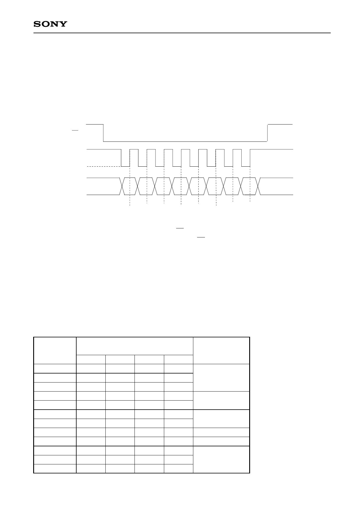
CS
SCK
SI
D0 D1 D2 D3 D4 D5 D6 D7
Fig. 1. Timing chart for the serial interface input block
Note) D0 to D7 internal transfer is completed by the CS signal switching from a Low to High pulse. Therefore,
the data should be transferred in 1-byte units with the CS signal reset each time.
• Description of mode switching settings using the serial interface
The CXD2436Q can set the following six modes.
(1) Frequency division ratio setting for the 1/N frequency divider of the master clock PLL circuit block.
(2) H screen center adjustment. The center changes by one dot with LSB.
(3) V screen center adjustment. The center changes by one line with LSB.
(4) Sample-and-hold circuit phase adjustment. The phase changes by a half-dot with LSB.
(See the Description of Sample-and-Hold Timing for details.)
(5) Clamp pulse timing adjustment (4-way)
(6) Data output (Serial data is held and output.)
Upper 4-bit
address value
Lower 4-bit data
Functions
D7 to D4
D3
D2
D1
D0
0H
PHP3 PHP2 PHP1 PHP0
PLL 1/N frequency
1H
PHP7 PHP6 PHP5 PHP4
divisions
2H
—
PHP10 PHP9 PHP8
3H
HP3
HP2
HP1
HP0
H screen center
4H
—
HP6
HP5
HP4
adjustment
5H
VP3
VP2
VP1
VP0
V screen center
6H
—
VP6
VP5
VP4
adjustment
7H
SHP3 SHP2 SHP1 SHP0 S/H timing
8H
—
—
CLPP1 CLPP0 Clamp timing
9H
PO3
PO2
PO1
PO0
AH
PO7
PO6
PO5
PO4 Data output
BH
PO11 PO10 PO9
PO8
∗ PHP0, HP0, VP0, SHP0, CLPP0
—11—
Share Link: 