HD74BC541A 데이터 시트보기 (PDF) - Renesas Electronics
부품명
상세내역
일치하는 목록
HD74BC541A Datasheet PDF : 8 Pages
| |||
HD74BC541A
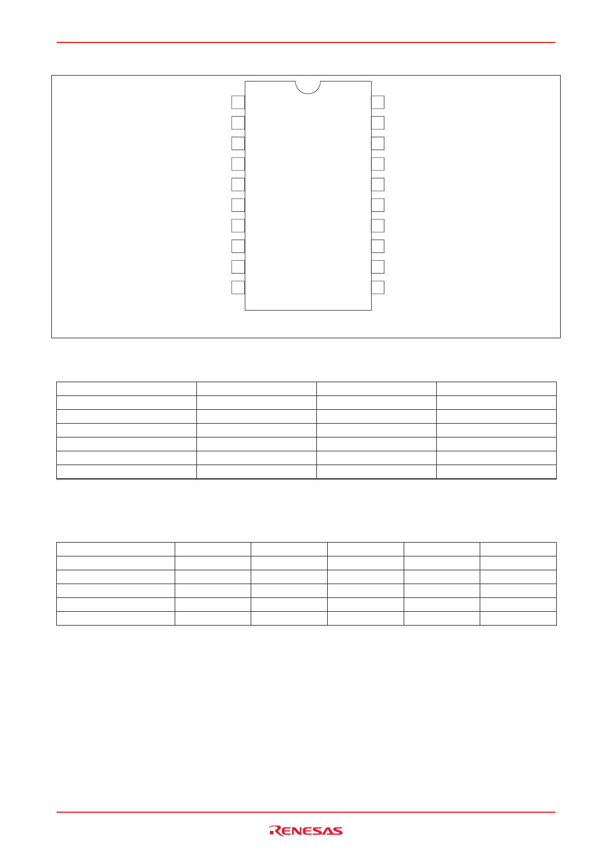
Pin Arrangement
G1 1
A1 2
A2 3
A3 4
A4
5
A5
6
A6
7
A7 8
A8
9
GND 10
20 VCC
19 G2
18 Y1
17 Y2
16 Y3
15 Y4
14 Y5
13 Y6
12 Y7
11 Y8
(Top view)
Absolute Maximum Ratings
Item
Symbol
Rating
Unit
Supply voltage
Input diode current
Input voltage
Output voltage
Off state output voltage
Storage temperature
VCC
IIK
VIN
VOUT
VOUT(off)
Tstg
–0.5 to +7.0
V
±30
mA
–0.5 to +7.5
V
–0.5 to +7.5
V
–0.5 to +5.5
V
–65 to +150
°C
Note: 1. The absolute maximum ratings are values which must not individually be exceeded, and furthermore, no two
of which may be realized at the same time.
Recommended Operating Conditions
Item
Symbol
Min
Typ
Supply voltage
VCC
4.5
5.0
Input voltage
VIN
0
—
Ouput voltage
VOUT
0
—
Operating temperature
Topr
–40
—
Input rise/fall time*1
tr , tf
0
—
Note: 1. This item guarantees maximum limit when one input switches.
Waveform: Refer to test circuit of switching characteristics.
Max
5.5
VCC
VCC
85
8
Unit
V
V
V
°C
ns/V
Rev.2.00, Jul.16.2004, page 2 of 7
Share Link: 