NCP1547(2007) 데이터 시트보기 (PDF) - ON Semiconductor
부품명
상세내역
일치하는 목록
NCP1547 Datasheet PDF : 13 Pages
| |||
NCP1547
duty cycle of the sync pulses can vary from 10% to 90%. The
frequency foldback feature is disabled during the sync
mode.
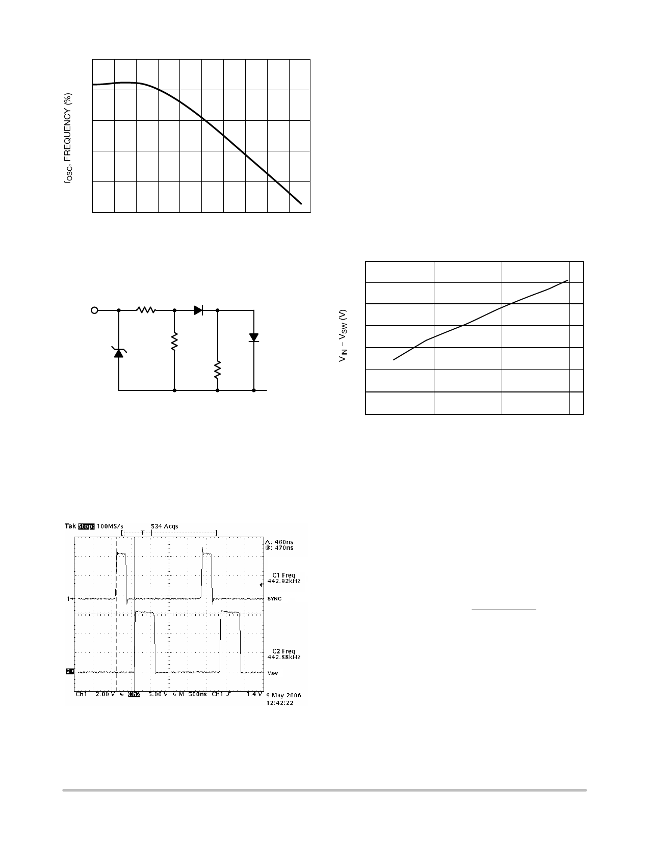
Figure 4. A NCP1547 Buck Regulator is
Synchronized to an External 443 kHz Pulse Signal
Power Switch and Current Limit
The collector of the built−in NPN power switch is
connected to the VIN pin, and the emitter to the VSW pin.
When the switch turns on, the VSW voltage is equal to the
VIN minus switch Saturation Voltage. In the buck regulator,
the VSW voltage swings to one diode drop below ground
when the power switch turns off, and the inductor current is
commutated to the catch diode. Due to the presence of high
pulsed current, the traces connecting the VSW pin, inductor
and diode should be kept as short as possible to minimize the
noise and radiation. For the same reason, the input capacitor
should be placed close to the VIN pin and the anode of the
diode.
The saturation voltage of the power switch is dependent
on the switching current, as shown in Figure 5.
0.7
0.6
0.5
0.4
0.3
0.2
0.1
0
0
0.5
1.0
1.5
SWITCHING CURRENT (A)
Figure 5. The Saturation Voltage of the Power Switch
Increases with the Conducting Current
The NCP1547 contains pulse−by−pulse current limiting
to protect the power switch and external components. When
the peak of the switching current reaches the Current Limit,
the power switch turns off after the Current Limit Delay. The
switch will not turn on until the next switching cycle. The
current limit threshold is independent of switching duty
cycle. The maximum load current, given by the following
formula under continuous conduction mode, is less than the
Current Limit due to the ripple current.
IO(MAX)
+
ILIM
*
VO(VIN * VO)
2(L)(VIN)(fs)
where:
fS = switching frequency,
ILIM = current limit threshold,
VO = output voltage,
VIN = input voltage,
L = inductor value.
When the regulator runs under current limit, the
subharmonic oscillation may cause low frequency
oscillation, as shown in Figure 6. Similar to current mode
control, this oscillation occurs at the duty cycle greater than
50% and can be alleviated by using a larger inductor value.
The current limit threshold is reduced to Foldback Current
when the FB pin falls below Foldback Threshold. This
feature protects the IC and external components under the
power up or over−load conditions.
Figure 6. The Regulator in Current Limit
BOOST Pin
The BOOST pin provides base driving current for the
power switch. A voltage higher than VIN provides required
headroom to turn on the power switch. This in turn reduces
IC power dissipation and improves overall system
efficiency. The BOOST pin can be connected to an external
boost−strapping circuit which typically uses a 0.1 mF capacitor
and a 1N914 or 1N4148 diode, as shown in Figure 1.
http://onsemi.com
7
Share Link: 