NCP1547(2007) 데이터 시트보기 (PDF) - ON Semiconductor
부품명
상세내역
일치하는 목록
NCP1547 Datasheet PDF : 13 Pages
| |||
NCP1547
APPLICATIONS INFORMATION
THEORY OF OPERATION
V2 Control
The NCP1547 buck regulator provides a high level of
integration and high operating frequencies allowing the
layout of a switch−mode power supply in a very small board
area. This device is based on the proprietary V2 control
architecture. V2 control uses the output voltage and its ripple
as the ramp signal, providing an ease of use not generally
associated with voltage or current mode control. Improved
line regulation, load regulation and very fast transient
response are also major advantages.
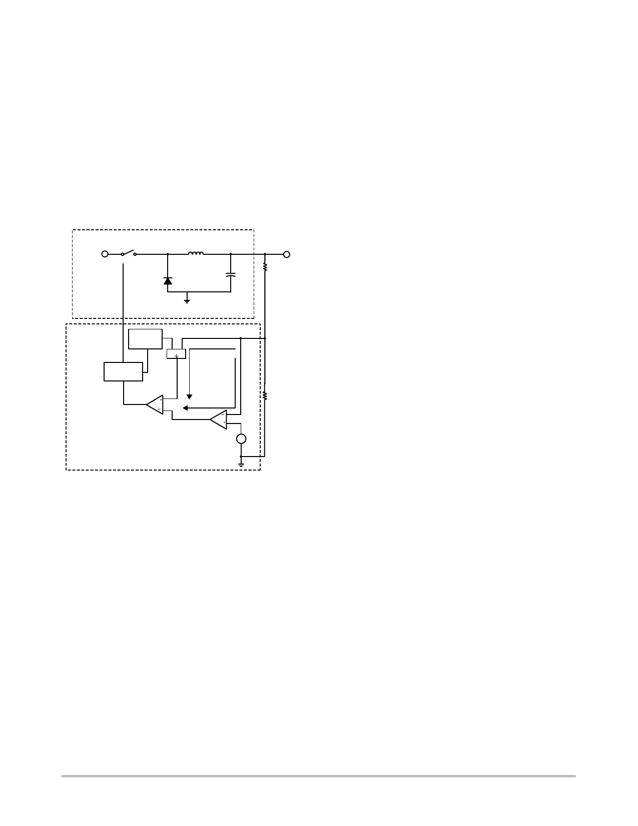
S1
L1
VIN
Duty Cycle
D1
VO
R1
C1
Buck
Controller
Slope
Oscillator Comp
FFB
Latch
R
S
PWM
Comparator
V2 Control
SFB
VC
Error
Amplifier
R2
VREF
+
−
Figure 3. Buck Converter with V2 Control.
As shown in Figure 3, there are two voltage feedback
paths in V2 control, namely FFB(Fast Feedback) and
SFB(Slow Feedback). In FFB path, the feedback voltage
connects directly to the PWM comparator. This feedback
path carries the ramp signal as well as the output DC voltage.
Artificial ramp derived from the oscillator is added to the
feedback signal to improve stability. The other feedback
path, SFB, connects the feedback voltage to the error
amplifier whose output VC feeds to the other input of the
PWM comparator. In a constant frequency mode, the
oscillator signal sets the output latch and turns on the switch
S1. This starts a new switch cycle. The ramp signal,
composed of both artificial ramp and output ripple,
eventually comes across the VC voltage, and consequently
resets the latch to turn off the switch. The switch S1 will turn
on again at the beginning of the next switch cycle. In a buck
converter, the output ripple is determined by the ripple
current of the inductor L1 and the ESR (equivalent series
resistor) of the output capacitor C1.
The slope compensation signal is a fixed voltage ramp
provided by the oscillator. Adding this signal eliminates
subharmonic oscillation associated with the operation at
duty cycle greater than 50%. The artificial ramp also ensures
the proper PWM function when the output ripple voltage is
inadequate. The slope compensation signal is properly sized
to serve it purposes without sacrificing the transient
response speed.
Under load and line transient, not only the ramp signal
changes, but more significantly the DC component of the
feedback voltage varies proportionally to the output voltage.
FFB path connects both signals directly to the PWM
comparator. This allows instant modulation of the duty cycle
to counteract any output voltage deviations. The transient
response time is independent of the error amplifier
bandwidth. This eliminates the delay associated with error
amplifier and greatly improves the transient response time.
The error amplifier is used here to ensure excellent DC
accuracy.
Error Amplifier
The NCP1547 has a transconductance error amplifier,
whose non−inverting input is connected to an Internal
Reference Voltage generated from the on−chip regulator.
The inverting input connects to the VFB pin. The output of
the error amplifier is made available at the VC pin. A typical
frequency compensation requires only a 0.1 mF capacitor
connected between the VC pin and ground, as shown in
Figure 1. This capacitor and error amplifier’s output
resistance (approximately 8.0 MW) create a low frequency
pole to limit the bandwidth. Since V2 control does not
require a high bandwidth error amplifier, the frequency
compensation is greatly simplified.
The VC pin is clamped below Output High Voltage. This
allows the regulator to recover quickly from over current or
short circuit conditions.
Oscillator and Sync Feature
The on−chip oscillator is trimmed at the factory and
requires no external components for frequency control. The
high switching frequency allows smaller external
components to be used, resulting in a board area and cost
savings. The tight frequency tolerance simplifies magnetic
components selection. The switching frequency is reduced
to 25% of the nominal value when the VFB pin voltage is
below Frequency Foldback Threshold. In short circuit or
over−load conditions, this reduces the power dissipation of
the IC and external components.
An external clock signal can sync the NCP1547 to a higher
frequency. The rising edge of the sync pulse turns on the
power switch to start a new switching cycle, as shown in
Figure 4. There is approximately 0.5 ms delay between the
rising edge of the sync pulse and rising edge of the VSW pin
voltage. The sync threshold is TTL logic compatible, and
http://onsemi.com
6
Share Link: 