NCP1547(2007) 데이터 시트보기 (PDF) - ON Semiconductor
부품명
상세내역
일치하는 목록
NCP1547 Datasheet PDF : 13 Pages
| |||
NCP1547
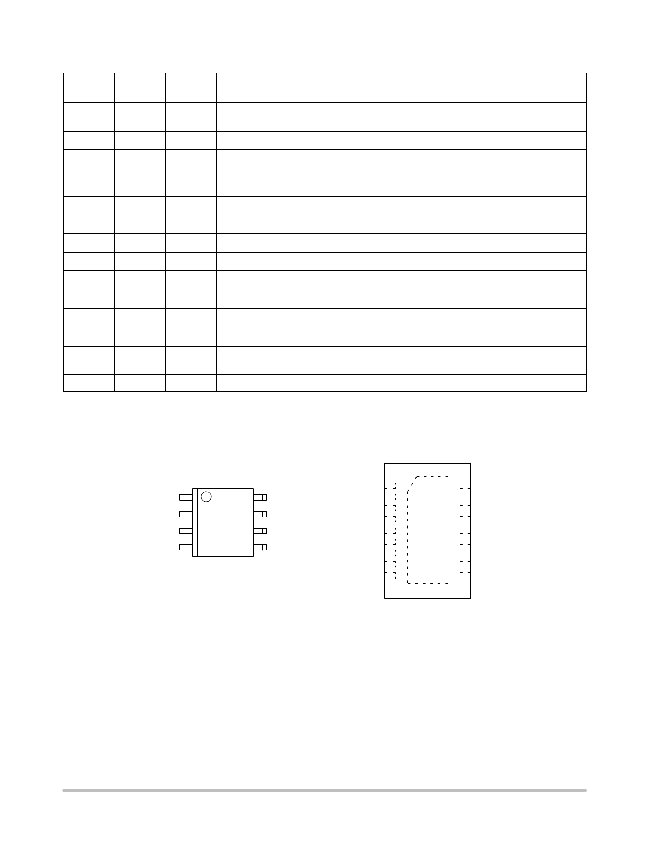
PACKAGE PIN DESCRIPTION
PIN NO.
PIN SYMBOL
FUNCTION
1
BOOST
The BOOST pin provides additional drive voltage to the on−chip NPN power transistor. The
resulting decrease in switch on voltage increases efficiency.
2
VIN
This pin is the main power input to the IC.
3
VSW
This is the connection to the emitter of the on−chip NPN power transistor and serves as the
switch output to the inductor. This pin may be subjected to negative voltages during switch off−
time. A catch diode is required to clamp the pin voltage in normal operation. This node can
stand −1.0 V for less than 50 ns during switch node flyback.
4
SHDNB
The shutdown pin is active low and TTL compatible. The IC goes into sleep mode, drawing less
than 1.0 mA when the pin voltage is pulled below 1.0 V.
This pin should be left floating in normal position.
5
SYNC
This pin provides the synchronization input.
6
GND
Power return connection for the IC.
7
VFB
The FB pin provides input to the inverting input of the error amplifier. If VFB is lower than 0.29 V,
the oscillator frequency is divided by four, and current limit folds back to about 1 A. These fea-
tures protect the IC under severe overcurrent or short circuit conditions.
8
VC
The VC pin provides a connection point to the output of the error amplifier and input to the PWM
comparator. Driving of this pin should be avoided because on−chip test circuitry becomes active
whenever current exceeding 0.5 mA is forced into the IC.
9, 11, 12, 14, 15, 18
NC
No Connection
PIN CONNECTIONS
BOOST 1
VIN
2
VIN
3
VIN
4
Vsw 5
VSW
6
VSW
7
SHDNB 8
NC 9
18 NC
17 VC
16
VFB
15 NC
14 NC
13 GND
12 NC
11 NC
10 SYNC
18−Lead DFN
http://onsemi.com
3
Share Link: 