74LVX374MSCX 데이터 시트보기 (PDF) - Fairchild Semiconductor
부품명
상세내역
일치하는 목록
74LVX374MSCX Datasheet PDF : 6 Pages
| |||
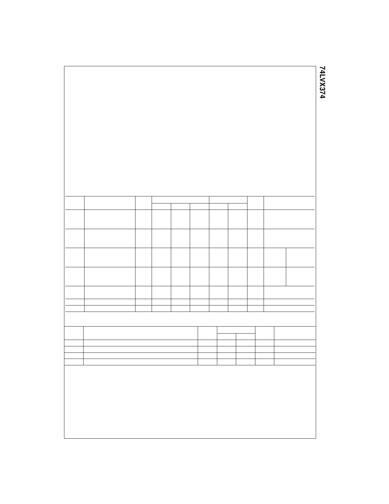
Absolute Maximum Ratings(Note 1)
Supply Voltage (VCC)
DC Input Diode Current (IIK)
VI = −0.5V
DC Input Voltage (VI)
DC Output Diode Current (IOK)
VO = −0.5V
VO = VCC +0.5V
DC Output Voltage (VO)
DC Output Source
or Sink Current (IO)
DC VCC or Ground Current
(ICC or IGND)
Storage Temperature (TSTG)
Power Dissipation
−0.5V to +7.0V
−20 mA
−0.5V to 7V
−20 mA
+20 mA
−0.5V to VCC + 0.5V
±25 mA
±75 mA
−65°C to +150°C
180mW
Recommended Operating
Conditions (Note 2)
Supply Voltage (VCC)
Input Voltage (VI)
Output Voltage (VO)
Operating Temperature (TA)
Input Rise and Fall Time (∆t/∆V)
2.0V to 3.6V
0V to 5.5V
0V to VCC
−40°C to +85°C
0 ns/V to 100 ns/V
Note 1: The “Absolute Maximum Ratings” are those values beyond which
the safety of the device cannot be guaranteed. The device should not be
operated at these limits. The parametric values defined in the Electrical
Characteristics tables are not guaranteed at the absolute maximum ratings.
The “Recommended Operating Conditions” table will define the conditions
for actual device operation.
Note 2: Unused inputs must be held HIGH or LOW. They may not float.
DC Electrical Characteristics
Symbol
Parameter
VCC
TA = +25°C
TA = −40°C to +85°C Units
Min
Typ
Max
Min
Max
Conditions
VIH
HIGH Level
Input Voltage
2.0
1.5
3.0
2.0
1.5
2.0
V
3.6
2.4
2.4
VIL
LOW Level
2.0
Input Voltage
3.0
0.5
0.5
0.8
0.8
V
3.6
0.8
0.8
VOH
HIGH Level
Output Voltage
2.0
1.9
3.0
2.9
3.0
2.58
VOL
LOW Level
2.0
Output Voltage
3.0
3.0
IOZ
3-STATE Output
3.6
Off-State Current
IIN
Input Leakage Current
3.6
ICC
Quiescent Supply Current
3.6
2.0
1.9
VIN = VIH IOH = − 50µA
3.0
2.9
V
or VIL IOH = −50µA
2.48
IOH = −4mA
0.0
0.1
0.1
VIN = VIH IOL = 50µA
0.0
0.1
0.1
V
or VIL IOL = 50µA
0.36
0.44
IOL = 4mA
±0.25
±2.5
VIN = VIH or VIL
µA VOUT = VCC or GND
±0.1
±1.0
µA VIN = 5.5V or GND
4.0
40.0
µA VIN = VCC or GND
Noise Characteristics (Note 3)
Symbol
Parameter
VOLP
Quiet Output Maximum Dynamic VOL
VOLV
Quiet Output Minimum Dynamic VOL
VIHD
Minimum HIGH Level Dynamic Input Voltage
VILD
Maximum LOW Level Dynamic Input Voltage
Note 3: Input tr = tf = 3 ns
VCC
TA = 25°C
Units
(V)
Typ
Limit
3.3
0.5
0.8
V
3.3
−0.5
−0.8
V
3.3
2.0
V
3.3
0.8
V
CL (pF)
50
50
50
50
3
www.fairchildsemi.com
Share Link: 