ICS94211 데이터 시트보기 (PDF) - Integrated Circuit Systems
부품명
상세내역
일치하는 목록
ICS94211 Datasheet PDF : 16 Pages
| |||
ICS94211
Absolute Maximum Ratings
Supply Voltage . . . . . . . . . . . . . . . . . . . . . . . . . . . . . 7.0 V
Logic Inputs . . . . . . . . . . . . . . . . . . . . . . . . . . . . . . . GND –0.5 V to VDD +0.5 V
Ambient Operating Temperature . . . . . . . . . . . . . . 0°C to +70°C
Case Temperature . . . . . . . . . . . . . . . . . . . . . . . . . . 115°C
Storage Temperature . . . . . . . . . . . . . . . . . . . . . . . . –65°C to +150°C
Stresses above those listed under Absolute Maximum Ratings may cause permanent damage to the device. These ratings are stress
specifications only and functional operation of the device at these or any other conditions above those listed in the operational sections
of the specifications is not implied. Exposure to absolute maximum rating conditions for extended periods may affect product
reliability.
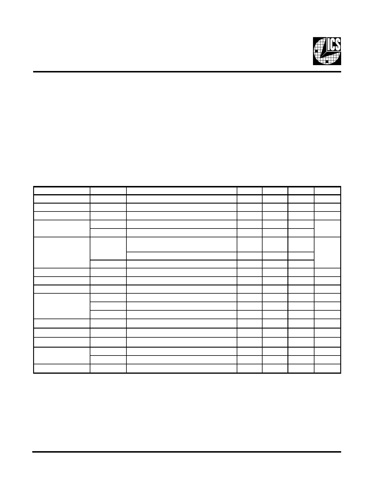
Electrical Characteristics - Input/Supply/Common Output Parameters
TA = 0 - 70C; Supply Voltage VDD = 3.3 V +/-5%, VDDL = 2.5 V +/-5% (unless otherwise stated)
PARAMETER SYMBOL
CONDITIONS
MIN TYP
MAX UNITS
Input High Voltage
Input Low Voltage
Input High Current
Input Low Current
Operating Supply
Current
VIH
VIL
IIH
IIL1
IIL2
IDD3.3OP
VIN = VDD
VIN = 0 V; Inputs with no pull-up resistors
VIN = 0 V; Inputs with pull-up resistors
CL = max cap loads;
CPU=66-133 MHz, SDRAM=100 MHz
CPU=133 MHz, SDRAM=133 MHz
2
VSS-0.3
-5
-5
-200
VDD+0.3
V
0.8
V
5
µA
µA
124
350
135
500
mA
Powerdown Current
Input Frequency
Pin Inductance
Input Capacitance1
Transition time1
Settling time1
Clk Stabilization1
Delay1
Skew1
IDD2.5OP
IDD3.3PD
Fi
Lpin
CIN
COUT
CINX
Ttrans
Ts
TSTAB
tPZH,tPZL
tPHZ,tPLZ
tcpu-pci
CL = max cap loads;
CL = 0 pF; Input address to VDD or GND
VDD = 3.3 V
Logic Inputs
Output pin capacitance
X1 & X2 pins
To 1st crossing of target frequency
From 1st crossing to 1% target frequency
From VDD = 3.3 V to 1% target frequency
Output enable delay (all outputs)
Output disable delay (all outputs)
VT = 1.5V; VTL=1.25V
18
70
600
14.318
7
5
6
27
45
3
3
3
1
10
1
10
2.45
4
µA
MHz
nH
pF
pF
pF
ms
ms
ms
ns
ns
ns
1Guaranteed by design, not 100% tested in production.
10
Share Link: 