84052IBZ 데이터 시트보기 (PDF) - Renesas Electronics
부품명
상세내역
일치하는 목록
84052IBZ Datasheet PDF : 19 Pages
| |||
ISL84051, ISL84052, ISL84053
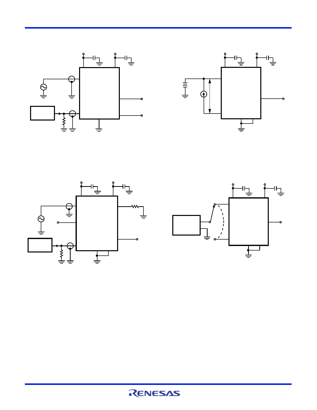
Test Circuits and Waveforms (Continued)
V+
C
V-
C
SIGNAL
GENERATOR
ANALYZER
RL
NO or NC
0V OR V+
ADDX
COM GND
0V OR V+
INH
V+
C
V-
C
rON = V1/1mA
NO or NC
VNX
1mA
V1
0V OR V+
ADDX
COM
GND INH
FIGURE 4. OFF ISOLATION TEST CIRCUIT
FIGURE 5. rON TEST CIRCUIT
V+
C
V-
C
SIGNAL
GENERATOR
0V OR V+
NOA or NCA COMA
ISL84052
AND
ADDX ISL84053
ANALYZER
RL
COMB
NOB or NCB
GND INH
50Ω
NC
FIGURE 6. CROSSTALK TEST CIRCUIT
Detailed Description
The ISL84051, ISL84052, ISL84053 analog switches offer
precise switching capability from a bipolar ±2V to ±6V or a
single 2V to 12V supply with low on-resistance (60Ω) and high
speed operation (tON = 50ns, tOFF = 40ns). The devices are
especially well suited to portable battery powered equipment
thanks to the low operating supply voltage (2V), low power
consumption (3µW), low leakage currents (5nA max). High
frequency applications also benefit from the wide bandwidth,
and the very high off isolation and crosstalk rejection.
Supply Sequencing And Overvoltage
Protection
With any CMOS device, proper power supply sequencing is
required to protect the device from excessive input currents
FN6047 Rev.10.00
May 16, 2011
IMPEDANCE
ANALYZER
V+
C
V-
C
NO OR NC
0V OR V+
ADDX
COM GND INH
FIGURE 7. CAPACITANCE TEST CIRCUIT
which might permanently damage the IC. All I/O pins contain
ESD protection diodes from the pin to V+ and to V- (see Figure
8). To prevent forward biasing these diodes, V+ and V- must be
applied before any input signals, and input signal voltages
must remain between V+ and V-. If these conditions cannot be
guaranteed, then one of the following two protection methods
should be employed.
Logic inputs can easily be protected by adding a 1kΩ resistor in
series with the input (see Figure 8). The resistor limits the input
current below the threshold that produces permanent
damage, and the sub-microamp input current produces an
insignificant voltage drop during normal operation.
This method is not applicable for the signal path inputs.
Adding a series resistor to the switch input defeats the purpose
of using a low rON switch, so two small signal diodes can be
Page 12 of 19
Share Link: 