EL7516IY 데이터 시트보기 (PDF) - Renesas Electronics
부품명
상세내역
일치하는 목록
EL7516IY Datasheet PDF : 12 Pages
| |||
EL7516
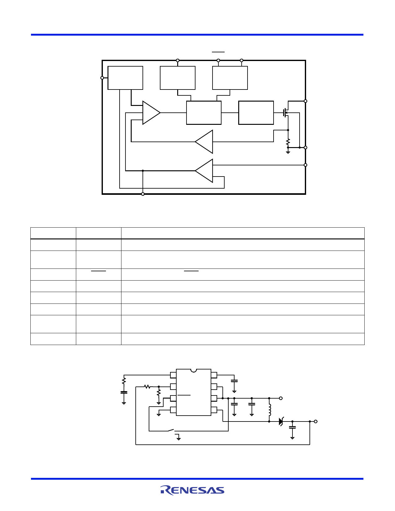
Block Diagram
VDD
REFERENCE
GENERATOR
FSEL
OSCILLATOR
SHDN
SS
SHUTDOWN
AND START-UP
CONTROL
COMPARATOR
PWM LOGIC
CONTROLLER
CURRENT
SENSE
COMP
GM
AMPLIFIER
FET
DRIVER
LX
GND
FB
Pin Descriptions
PIN NUMBER
PIN NAME
1
COMP
2
FB
3
SHDN
4
GND
5
LX
6
VDD
7
FSEL
8
SS
DESCRIPTION
Compensation pin. Output of the internal error amplifier. Capacitor and resistor from COMP pin to ground.
Voltage feedback pin. Internal reference is 1.294V nominal. Connect a resistor divider from VOUT. VOUT =
1.294V (1 + R1/R2). See Typical Application Circuit.
Shutdown control pin. Pull SHDN low to turn off the device.
Analog and power ground.
Power switch pin. Connected to the drain of the internal power MOSFET.
Analog power supply input pin.
Frequency select pin. When FSEL is set low, switching frequency is set to 620kHz. When connected to
high or VDD, switching frequency is set to 1.25MHz.
Soft-start control pin. Connect a capacitor to control the converter start-up.
Typical Application Circuit
R3
3.9k
C5
4.7nF
R1 85.2k
R2
10k
1 COMP
2 FB
3 SHDN
SS 8
FSEL 7
VDD 6
4 GND
LX 5
S1
C3
27nF
C4 + C1
0.1µF 22µF
2.7V TO 5.5V
10µH
D1
+ C2
22µF
12V
FN7333 Rev 6.00
October 9, 2007
Page 3 of 12
Share Link: 