KC7050B-C3(V2) 데이터 시트보기 (PDF) - Kyocera Kinseki Corpotation
부품명
상세내역
일치하는 목록
KC7050B-C3
(Rev.:V2)
(Rev.:V2)
Kyocera Kinseki Corpotation

KC7050B-C3 Datasheet PDF : 1 Pages
| |||
Clock Oscillators Surface Mount Type
KC7050B Series (FXO-31F Series)
CMOS/ 3.3V/ 5.0V/ 7.0×5.0mm
RoHS Compliant
Features
• Surface mount type suitable for auto
pick-and-place
• Reflow soldering compatible
• CMOS, TTL IC direct drive is possible
• With tri-state function
• B road frequency range from 1.8MHz to 50MHz
• Supply voltage VCC=3.3/ 5.0V available
Frequency Tolerance (Overall)
Freq. Tol. Operating
Code
× 10-6
Temperature
Range (°C)
1
0
S
±100
± 50
± 30
-10 to +70
(Standard)
Note
1.8 to 50MHz
1.8 to 33MHz
How to Order
KC7050B 25.0000 C 3 1 A 00
①
② ③④⑤⑥ ⑦
① Type
② Output Frequency
③ Output Type (CMOS)
④ Supply Voltage 5=5.0V, 3=3.3V
⑤ Frequency Tolerance (See Table at Left)
⑥ S ymmetry/ INH Function
A: 40/ 60%, Disable
B: 40/ 60%, Stand-by
⑦ C ustomer Special Model Suffix
(STD Specification is “00”)
Symmetry/ INH Function
Freq.
(MHz)
1.8 to 39.9
40 to 50
Code
KC7050B-C5 KC7050B-C3
A
A
A
B
Specifications
Item
Output Frequency Range
Symbol
fo
Frequency Tolerance (Overall) f_tol
Storage Temperature Range
Operating Temperature Range
Max. Supply Voltage
Supply Voltage
T_stg
T_use
—
VCC
Current Consumption
ICC
Stand-by/ Disable Current
Symmetry
Rise/ Fall Time
Low Level Output Voltage
High Level Output Voltage
CMOS Load
Input Voltage Range
Low Level Input Voltage
High Level Input Voltage
Disable Time
Enable Time
Start-up Time
I_std
SYM
tr/ tf
VOL
VOH
L_CMOS
VIN
VIL
VIH
t_dis
t_ena
t_str
Conditions
KC7050Bxx.xxxxC5xA00 (FXO-31FH) KC7050Bxx.xxxxC3xx00 (FXO-31FL)
1.8 to 50
±30 (to 33MHz)
±50 (to 33MHz)
±100 (to 50MHz)
-40 to +85
-10 to +70
7 max.
5±0.5
3.3±0.3
25 max. (1.8 to 15MHz)
30 max. (15.1 to 32MHz)
45 max. (32.1 to 50MHz)
18 max. (1.8 to 39.9MHz)
25 max. (40 to 50MHz)
10 max.
40 to 60@50%VCC
10 max.
10% VCC max.
90% VCC min.
50 max.
20 max.
0 to VCC
0 to VCC
0.8 max.
0.3 max.
2.2 min.
2.2 min.
150 max.
5 max.
10 max.
Note: A ll electrical characteristics are defined at the maximum load and operating temperature range.
Please contact us for inquiry about operating temperature range, available frequencies and other conditions.
Units
MHz
×10-6
°C
°C
V
V
mA
μA
%
ns
V
V
pF
V
V
V
ns
ms
ms
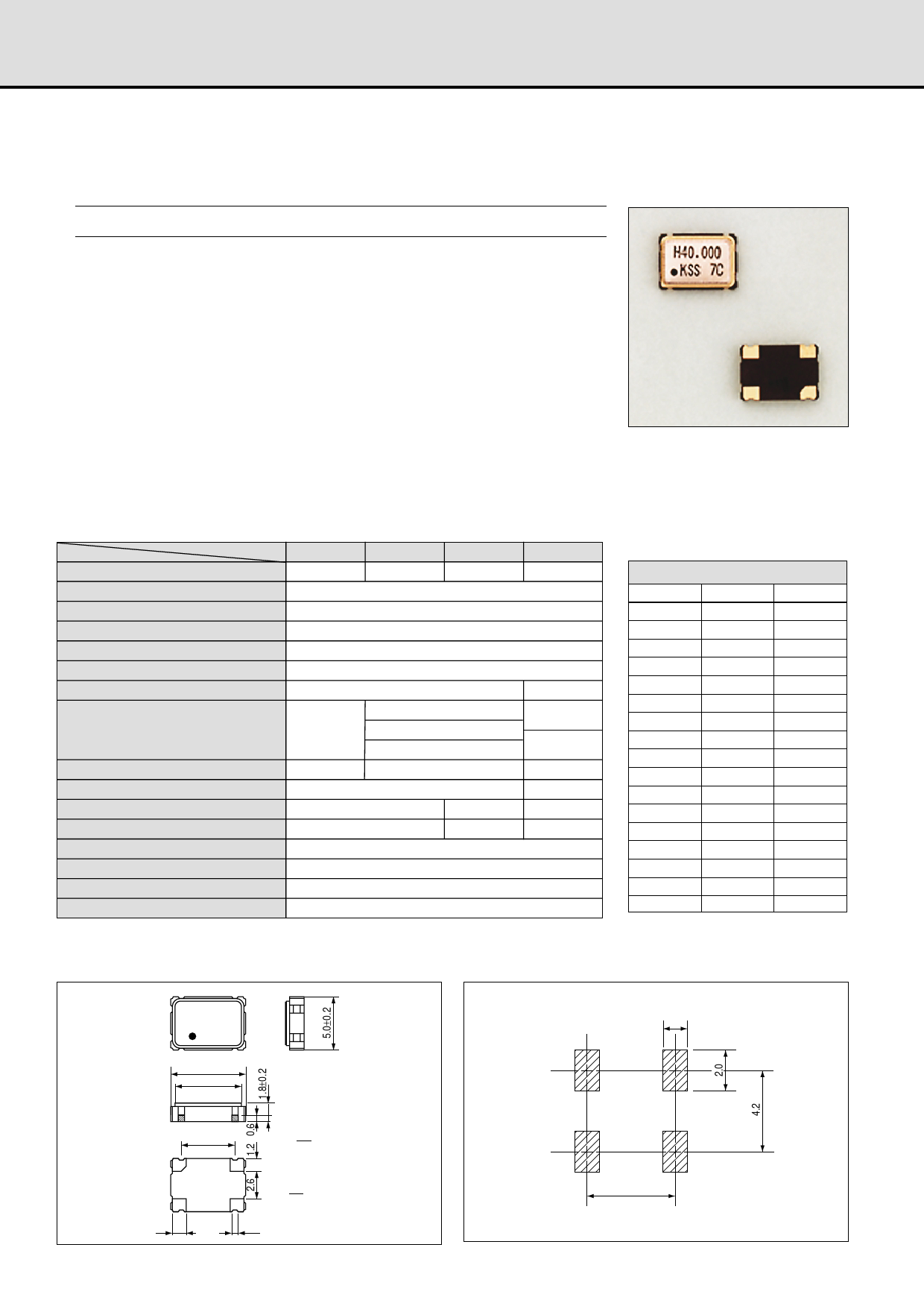
Dimensions
7.0
0.6
1.4
#3 #4
#2 #1
5.1
Plating: Ni+Au
Tolerance: ±0.2
(Unit: mm) Recommended Land Pattern (Unit: mm)
5.1
Pad Connections
#1 INH
#2 GND
#3 Output
#4 VCC
INH Function
Pad1
Pad3 (Output)
Open
Active
"H" Level
Active
"L" Level High Z (Output-Stop)
1.8
Note: A capacitor of value 0.01µF between VCC
and GND is recommended.
Share Link: