CY7C146(2005) 데이터 시트보기 (PDF) - Cypress Semiconductor
부품명
상세내역
일치하는 목록
CY7C146 Datasheet PDF : 18 Pages
| |||
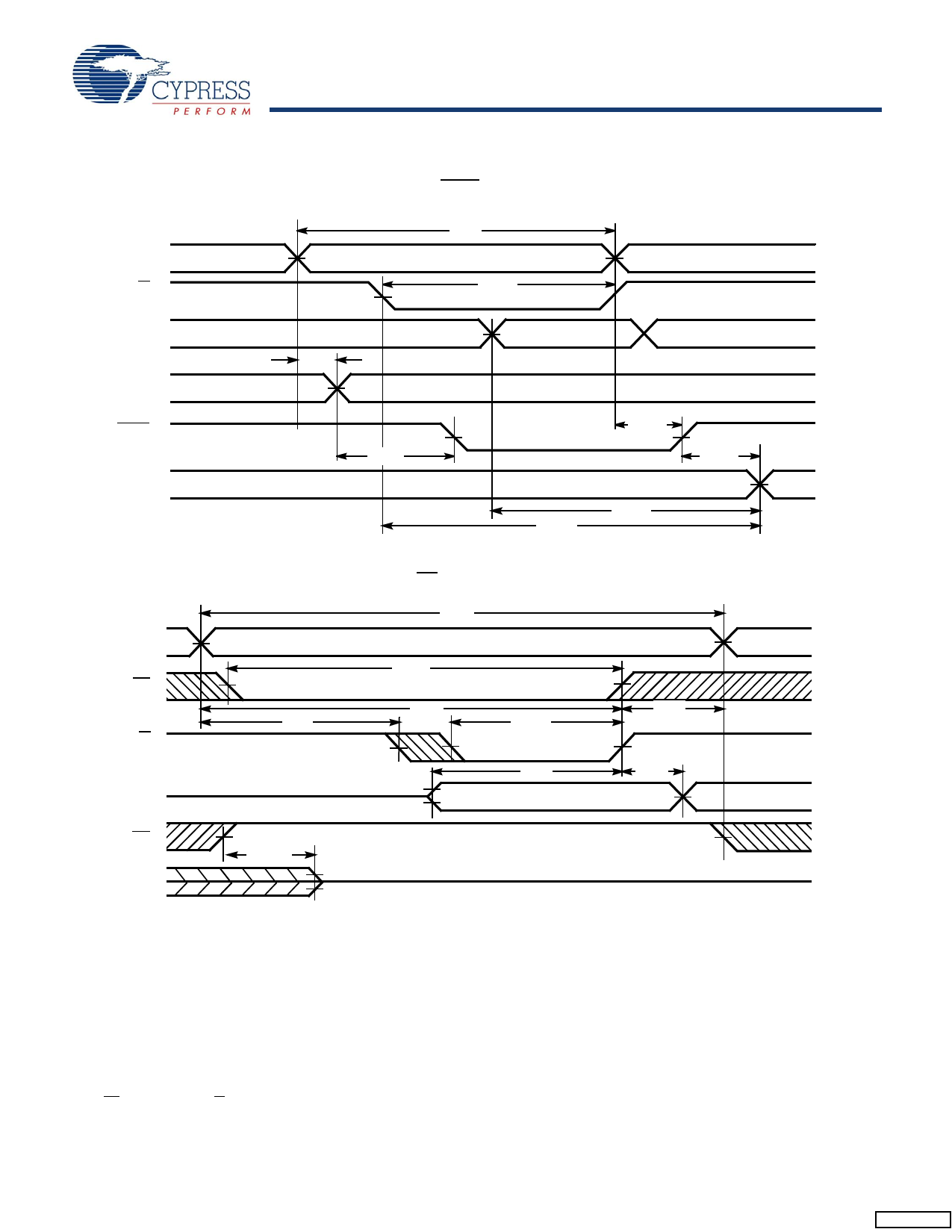
Switching Waveforms (continued)
Write Cycle No.1 (OE Three-States Data I/Os—Either Port)[14, 22]
ADDRESS
CE
R/W
DATAIN
tWC
tSCE
tAW
tSA
tPWE
tSD
DATA VALID
CY7C132/CY7C136
CY7C142/CY7C146
tHA
tHD
OE
DOUT
tHZOE
HIGH IMPEDANCE
Write Cycle No. 2 (R/W Three-States Data I/Os—Either Port)[14, 23]
ADDRESS
CE
R/W
DATAIN
DOUT
tWC
tSCE
tHA
tAW
tSA
tPWE
tHZWE
tSD
tHD
DATA VALID
tLZWE
HIGH IMPEDANCE
Notes:
22. If OE is LOW during a R/W controlled write cycle, the write pulse width must be the larger of tPWE or tHZWE + tSD to allow the data I/O pins to enter high impedance
and for data to be placed on the bus for the required tSD.
23. If the CE LOW transition occurs simultaneously with or after the R/W LOW transition, the outputs remain in a high-impedance state.
Document #: 38-06031 Rev. *C
Page 8 of 18
Share Link: 