ISL97642 데이터 시트보기 (PDF) - Renesas Electronics
부품명
상세내역
일치하는 목록
ISL97642 Datasheet PDF : 19 Pages
| |||
ISL97642
FBB
CINT
DRVN
FBN
VREF REFERENCE
GENERATOR
OSCILLATOR
SLOPE COMP OSC
COMPENSATION
PWM
LOGIC
CONTROLLER
GM
AMPLIFIER
BUFFER
UVLO
COMPARATOR
THERMAL
SHUTDOWN
CURRENT
AMPLIFIER
SHUTDOWN
AND START-UP
CONTROL
CURRENT REF
CURRENT
LIMIT COMPARATOR
SS
VREF
+
-
UVLO
COMPARATOR
BUFFER
SS
+ 0.2V
-
0.4V
UVLO
COMPARATOR
BUFFER
LX
PGND
DRVP
FBP
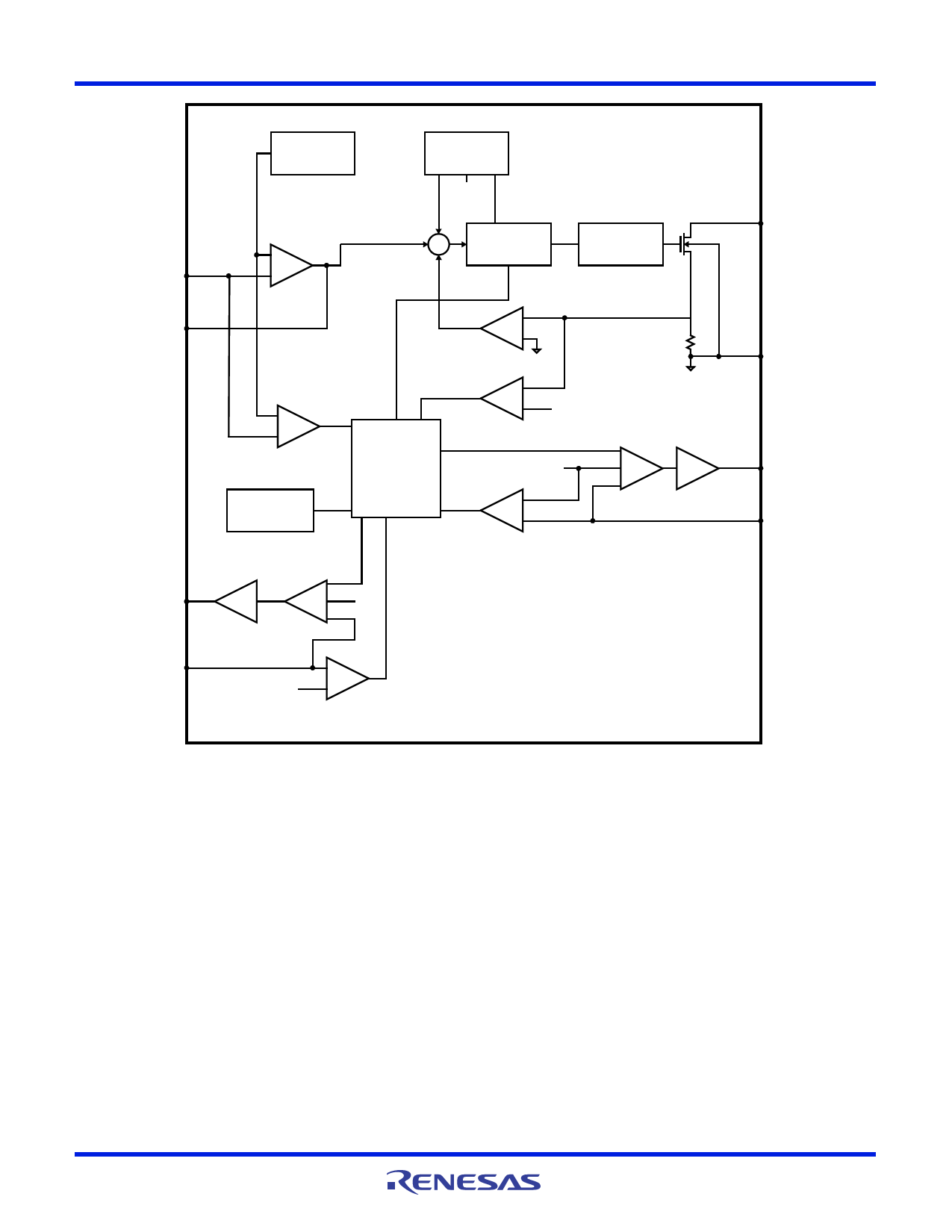
FIGURE 16. BLOCK DIAGRAM
Boost Converter
The main boost converter is a current mode PWM converter
operating at a fixed frequency. The 1.2MHz switching
frequency enables the use of low profile inductor and
multilayer ceramic capacitors, which results in a compact, low
cost power system for LCD panel design.
The boost converter can operate in continuous or
discontinuous inductor current mode. The ISL97642 is
designed for continuous current mode, but it can also operate
in discontinuous current mode at light load. In continuous
current mode, current flows continuously in the inductor during
the entire switching cycle in steady state operation. The
voltage conversion ratio in continuous current mode is given by
Equation 1:
V-----B---V-O---I-O-N----S----T- = 1-----–-1----D---
(EQ. 1)
Figure 17 shows the block diagram of the boost controller.
It uses a summing amplifier architecture consisting of GM
stages for voltage feedback, current feedback and slope
compensation. A comparator looks at the peak inductor current
cycle by cycle and terminates the PWM cycle if the current limit
is reached.
An external resistor divider is required to divide the output
voltage down to the nominal reference voltage. Current drawn
by the resistor network should be limited to maintain the overall
converter efficiency. The maximum value of the resistor network
is limited by the feedback input bias current and the potential for
noise being coupled into the feedback pin. A resistor network in
the order of 60k is recommended. The boost converter output
voltage is determined using Equation 2:
VBOOST = R-----1--R--+---1--R-----2- VREF
(EQ. 2)
Where D is the duty cycle of switching MOSFET.
FN6436 Rev 0.00
June 18, 2007
Page 10 of 19
Share Link: 