ADSP-2171 데이터 시트보기 (PDF) - Analog Devices
부품명
상세내역
일치하는 목록
ADSP-2171 Datasheet PDF : 52 Pages
| |||
ADSP-2171/ADSP-2172/ADSP-2173
CLOCK OR
CRYSTAL
6
9
4
7
16
CLKIN
CLKOUT
XTAL
RESET
PWD PWDACK
VDD
GND
HOST
MODE
HIP
SERIAL
PORT 0
IRQ2
ADSP-217x
BR
BG
MMAP
3
FL2-0
PMS
RD
WR
ADDRESS DATA
SERIAL
PORT 1
DMS
BMS
14
24
HIP CONTROL
HIP DATA/ADDR
SCLK
RFS
TFS
DT
DR
SCLK
RFS or IRQ0
TFS or IRQ1
DT or FO
DR or FI
HOST
PROCESSOR
(OPTIONAL)
SERIAL DEVICE
(OPTIONAL)
SERIAL DEVICE
(OPTIONAL)
24
A
D
CS
PROGRAM OE
MEMORY
(OPTIONAL)
WE
D23-8
14
16
A
D
CS
DATA MEMORY
OE
&
WE PERIPHERALS
OE
(OPTIONAL)
NOTE:
THE TWO MSBs OF THE DATA BUS ARE USED AS THE MSBs OF THE BOOT EPROM ADDRESS.
THIS IS ONLY REQUIRED FOR THE 27C256 AND 27C512.
D23-22
2
D15-8
8
A
D
CS
BOOT MEMORY
e.g., EPROM
27C64
27C128
27C256
27C512
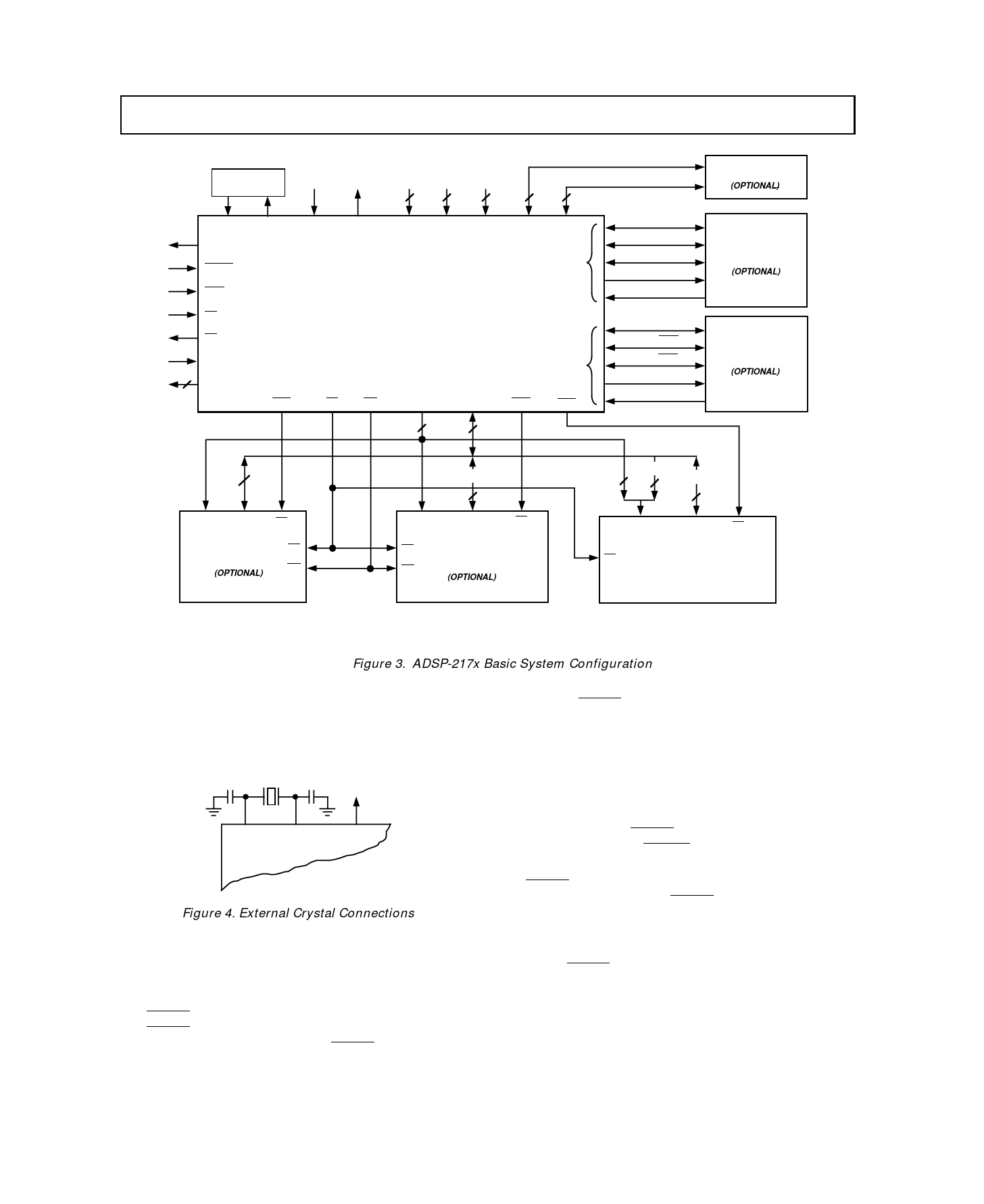
Figure 3. ADSP-217x Basic System Configuration
Because the ADSP-217x includes an on-chip oscillator circuit,
an external crystal may be used. The crystal should be con-
nected across the CLKIN and XTAL pins, with two capacitors
connected as shown in Figure 4. A parallel-resonant, fundamen-
tal frequency, microprocessor-grade crystal should be used.
CLKIN
XTAL
ADSP-217x
CLKOUT
Figure 4. External Crystal Connections
A clock output (CLKOUT) signal is generated by the processor
at the processor’s cycle rate. This can be enabled and disabled
by the CLKODIS bit in the SPORT0 Autobuffer Control Reg-
ister, DM[0x3FF3].
Reset
The RESET signal initiates a master reset of the ADSP-217x.
The RESET signal must be asserted during the power-up se-
quence to assure proper initialization. RESET during initial
power-up must be held long enough to allow the internal clock
to stabilize. If RESET is activated any time after power-up, the
clock continues to run and does not require stabilization time.
The power-up sequence is defined as the total time required for
the crystal oscillator circuit to stabilize after a valid VDD is ap-
plied to the processor, and for the internal phase-locked loop
(PLL) to lock onto the specific crystal frequency. A minimum of
2000 CLKIN cycles ensures that the PLL has locked but does
not include the crystal oscillator start-up time. During this
power-up sequence the RESET signal should be held low. On
any subsequent resets, the RESET signal must meet the mini-
mum pulse width specification, tRSP.
The RESET input contains some hysteresis; however, if you use
an RC circuit to generate your RESET signal, the use of an ex-
ternal Schmidt trigger is recommended.
The master reset sets all internal stack pointers to the empty
stack condition, masks all interrupts and clears the MSTAT reg-
ister. When RESET is released, if there is no pending bus re-
quest and the chip is configured for booting (MMAP = 0), the
boot-loading sequence is performed. Then the first instruction is
fetched from internal program memory location 0x0000.
REV. A
–7–
Share Link: 