MC74VHC595 데이터 시트보기 (PDF) - ON Semiconductor
부품명
상세내역
일치하는 목록
MC74VHC595 Datasheet PDF : 11 Pages
| |||
MC74VHC595
8-Bit Shift Register with
Output Storage Register
(3-State)
The MC74VHC595 is an advanced high speed 8−bit shift register
with an output storage register fabricated with silicon gate CMOS
technology.
It achieves high speed operation similar to equivalent Bipolar
Schottky TTL while maintaining CMOS low power dissipation.
The MC74VHC595 contains an 8−bit static shift register which
feeds an 8−bit storage register.
Shift operation is accomplished on the positive going transition of
the Shift Clock input (SCK). The output register is loaded with the
contents of the shift register on the positive going transition of the
Register Clock input (RCK). Since the RCK and SCK signals are
independent, parallel outputs can be held stable during the shift
operation. And, since the parallel outputs are 3−state, the VHC595 can
be directly connected to an 8−bit bus. This register can be used in
serial−to−parallel conversion, data receivers, etc.
The internal circuit is composed of three stages, including a buffer
output which provides high noise immunity and stable output. The
inputs tolerate voltages up to 7 V, allowing the interface of 5 V systems
to 3 V systems.
Features
• High Speed: fmax = 185 MHz (Typ) at VCC = 5 V
• Low Power Dissipation: ICC = 4 mA (Max) at TA = 25°C
• High Noise Immunity: VNIH = VNIL = 28% VCC
• Power Down Protection Provided on Inputs
• Balanced Propagation Delays
• Designed for 2 V to 5.5 V Operating Range
• Low Noise: VOLP = 1.0 V (Max)
• Pin and Function Compatible with Other Standard Logic Families
• Latchup Performance Exceeds 300 mA
• ESD Performance: HBM > 2000 V; Machine Model > 200 V
• NLV Prefix for Automotive and Other Applications Requiring
Unique Site and Control Change Requirements; AEC−Q100
Qualified and PPAP Capable
• These Devices are Pb−Free and are RoHS Compliant
© Semiconductor Components Industries, LLC, 2015
1
February, 2015 − Rev. 6
www.onsemi.com
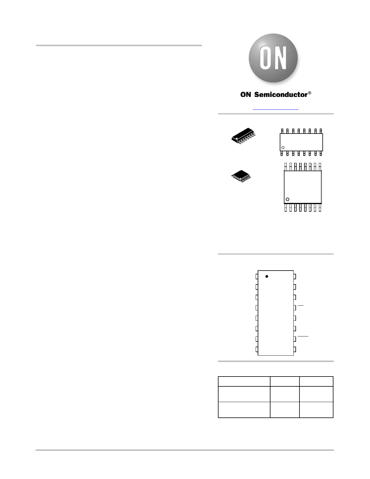
MARKING DIAGRAMS
SOIC−16
D SUFFIX
CASE 751B
TSSOP−16
DT SUFFIX
CASE 948F
16
9
VHC595G
AWLYWW
1
8
16
9
VHC
595
ALYWG
G
1
8
A
= Assembly Location
WL = Wafer Lot
Y
= Year
W, WW = Work Week
G or G = Pb−Free Package
(Note: Microdot may be in either location)
PIN ASSIGNMENT
QB 1
QC 2
QD 3
QE 4
QF 5
QG 6
QH 7
GND 8
16 VCC
15 QA
14 SI
13 OE
12 RCK
11 SCK
10 SCLR
9 SQH
ORDERING INFORMATION
Device
Package Shipping†
MC74VHC595DR2G SOIC−16 2500 Tape &
(Pb−Free)
Reel
MC74VHC595DTR2G, TSSOP−16 2500 Tape &
NLV74VHC595DTR2G (Pb−Free)
Reel
†For information on tape and reel specifications,
including part orientation and tape sizes, please
refer to our Tape and Reel Packaging Specification
Brochure, BRD8011/D.
Publication Order Number:
MC74VHC595/D
Share Link: 