SAA7108AE 데이터 시트보기 (PDF) - NXP Semiconductors.
부품명
상세내역
일치하는 목록
SAA7108AE Datasheet PDF : 208 Pages
| |||
NXP Semiconductors
SAA7108AE; SAA7109AE
HD-CODEC
6
Gv
(dB)
0
−6
mgb706
−12
−18
−24
−30
−36
−42
−48
−54
0
2
4
6
8
10
12
14
f (MHz)
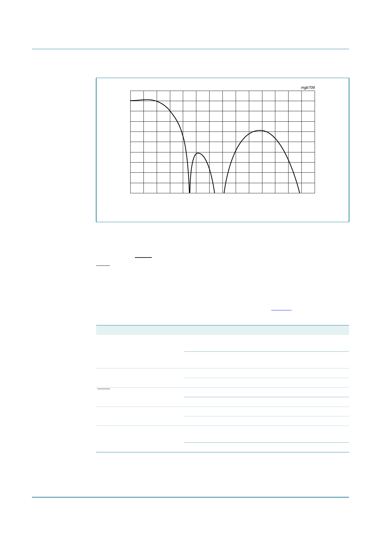
Fig 11. Color difference transfer characteristic in RGB (excluding scaler)
8.1 Reset conditions
To activate the reset, a pulse of at least 2 crystal clocks duration is required.
During reset (RESe = LOW) plus an extra 32 crystal clock periods, FSVGC, VSVGC,
CBO, HSVGC and TTX_SRES are set to input mode and HSM_CSYNC and VSM are set
to 3-state. A reset also forces the I2C-bus interface to abort any running bus transfer and
sets it into receive condition.
After reset, the state of the I/Os and other functions is defined by the strapping pins until
an I2C-bus access redefines the corresponding registers; see Table 5.
Table 5. Strapping pins
Pin
FSVGC (pin G1)
VSVGC (pin F1)
CBO (pin G3)
HSVGC (pin E3)
TTXRQ_XCLKO2 (pin C4)
Tied
LOW
HIGH
LOW
HIGH
LOW
HIGH
LOW
HIGH
LOW
HIGH
Preset
NTSC M encoding, PIXCLK fits to 640 × 480
graphics input
PAL B/G encoding, PIXCLK fits to 640 × 480
graphics input
4 : 2 : 2 Y-CB-CR graphics input (format 0)
4 : 4 : 4 RGB graphics input (format 3)
input demultiplex phase: LSB = LOW
input demultiplex phase: LSB = HIGH
input demultiplex phase: MSB = LOW
input demultiplex phase: MSB = HIGH
slave (FSVGC, VSVGC and HSVGC are inputs,
internal color bar is active)
master (FSVGC, VSVGC and HSVGC are outputs)
SAA7108AE_SAA7109AE_3
Product data sheet
Rev. 03 — 6 February 2007
© NXP B.V. 2007. All rights reserved.
20 of 208
Share Link: 