MC74HCT373ADTR2G 데이터 시트보기 (PDF) - ON Semiconductor
부품명
상세내역
일치하는 목록
MC74HCT373ADTR2G
ON Semiconductor

MC74HCT373ADTR2G Datasheet PDF : 9 Pages
| |||
MC74HCT373A
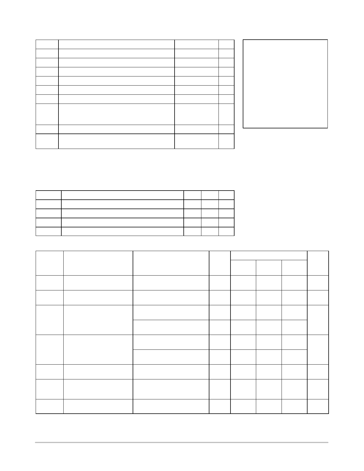
ÎÎÎÎÎÎÎÎÎÎÎÎÎÎÎÎÎÎÎÎÎÎÎ MAXIMUM RATINGS*
ÎÎÎÎÎÎÎÎÎÎÎÎÎÎÎÎÎÎÎÎÎÎÎ Symbol
Parameter
Value
Unit
ÎÎÎÎÎÎÎÎÎÎÎÎÎÎÎÎÎÎÎÎÎÎÎ VCC DC Supply Voltage (Referenced to GND)
– 0.5 to + 7.0
V
ÎÎÎÎÎÎÎÎÎÎÎÎÎÎÎÎÎÎÎÎÎÎÎ Vin DC Input Voltage (Referenced to GND)
– 0.5 to VCC + 0.5 V
ÎÎÎÎÎÎÎÎÎÎÎÎÎÎÎÎÎÎÎÎÎÎÎ Vout DC Output Voltage (Referenced to GND)
– 0.5 to VCC + 0.5 V
ÎÎÎÎÎÎÎÎÎÎÎÎÎÎÎÎÎÎÎÎÎÎÎ Iin
DC Input Current, per Pin
± 20
mA
ÎÎÎÎÎÎÎÎÎÎÎÎÎÎÎÎÎÎÎÎÎÎÎ Iout DC Output Current, per Pin
± 35
mA
ÎÎÎÎÎÎÎÎÎÎÎÎÎÎÎÎÎÎÎÎÎÎÎ ICC DC Supply Current, VCC and GND Pins
± 75
mA
ÎÎÎÎÎÎÎÎÎÎÎÎÎÎÎÎÎÎÎÎÎÎÎ PD Power Dissipation in Still Air,
Plastic DIP†
750
mW
SOIC Package†
500
ÎÎÎÎÎÎÎÎÎÎÎÎÎÎÎÎÎÎÎÎÎÎÎ TSSOP Package†
450
ÎÎÎÎÎÎÎÎÎÎÎÎÎÎÎÎÎÎÎÎÎÎÎ Tstg Storage Temperature
– 65 to + 150
°C
ÎÎÎÎÎÎÎÎÎÎÎÎÎÎÎÎÎÎÎÎÎÎÎ TL Lead Temperature, 1 mm from Case for 10 Seconds
°C
ÎÎÎÎÎÎÎÎÎÎÎÎÎÎÎÎÎÎÎÎÎÎÎ (Plastic DIP, SOIC, SSOP or TSSOP Package)
260
ÎÎÎÎÎÎÎÎÎÎÎÎÎÎÎÎÎÎÎÎÎÎÎ *Maximum Ratings are those values beyond which damage to the device may occur.
Functional operation should be restricted to the Recommended Operating Conditions.
†Derating — Plastic DIP: – 10 mW/°C from 65° to 125°C
SOIC Package: – 7 mW/°C from 65° to 125°C
TSSOP Package: − 6.1 mW/°C from 65° to 125°C
RECOMMENDED OPERATING CONDITIONS
ÎÎÎÎÎÎÎÎÎÎÎÎÎÎÎÎÎÎÎÎÎÎÎ Symbol
Parameter
Min Max Unit
ÎÎÎÎÎÎÎÎÎÎÎÎÎÎÎÎÎÎÎÎÎÎÎ VCC
DC Supply Voltage (Referenced to GND)
4.5 5.5 V
ÎÎÎÎÎÎÎÎÎÎÎÎÎÎÎÎÎÎÎÎÎÎÎ Vin, Vout DC Input Voltage, Output Voltage (Referenced to GND) 0
VCC
V
ÎÎÎÎÎÎÎÎÎÎÎÎÎÎÎÎÎÎÎÎÎÎÎ TA
Operating Temperature, All Package Types
– 55 + 125 °C
ÎÎÎÎÎÎÎÎÎÎÎÎÎÎÎÎÎÎÎÎÎÎÎÎÎÎÎÎÎÎÎÎÎÎÎÎÎÎÎÎÎÎÎÎÎÎ tr, tf
Input Rise and Fall Time (Figure 1)
0 500 ns
This device contains protection
circuitry to guard against damage
due to high static voltages or electric
fields. However, precautions must
be taken to avoid applications of any
voltage higher than maximum rated
voltages to this high−impedance cir-
cuit. For proper operation, Vin and
Vout should be constrained to the
range GND v (Vin or Vout) v VCC.
Unused inputs must always be
tied to an appropriate logic voltage
level (e.g., either GND or VCC).
Unused outputs must be left open.
DC ELECTRICAL CHARACTERISTICS (Voltages Referenced to GND)
ÎÎÎÎÎÎÎÎÎÎÎÎÎÎÎÎÎÎÎÎÎÎÎÎÎÎÎÎÎÎÎÎÎÎÎÎÎÎÎÎÎÎÎÎÎÎÎÎÎÎÎÎÎÎÎÎÎÎÎÎÎÎÎÎÎÎ Symbol
Parameter
VCC
Test Conditions
V
ÎÎÎÎÎÎÎÎÎÎÎÎÎÎÎÎÎÎÎÎÎÎÎÎÎÎÎÎÎÎÎÎÎÎÎÎÎÎÎÎÎÎÎÎÎÎÎÎÎÎÎÎÎÎÎÎÎÎÎÎÎÎÎÎÎÎ VIH
Minimum High−Level Input
Vout = 0.1 V or VCC – 0.1 V
4.5
Voltage
|Iout| v 20 mA
5.5
ÎÎÎÎÎÎÎÎÎÎÎÎÎÎÎÎÎÎÎÎÎÎÎÎÎÎÎÎÎÎÎÎÎ VIL
Maximum Low−Level Input
Vout = 0.1 V or VCC – 0.1 V
4.5
ÎÎÎÎÎÎÎÎÎÎÎÎÎÎÎÎÎÎÎÎÎÎÎÎÎÎÎÎÎÎÎÎÎ Voltage
|Iout| v 20 mA
5.5
ÎÎÎÎÎÎÎÎÎÎÎÎÎÎÎÎÎÎÎÎÎÎÎÎÎÎÎÎÎÎÎÎÎ VOH
Minimum High−Level Output Vin = VIH or VIL
4.5
Voltage
|Iout| v 20 mA
5.5
ÎÎÎÎÎÎÎÎÎÎÎÎÎÎÎÎÎÎÎÎÎÎÎÎÎÎÎÎÎÎÎÎÎ Vin = VIH or VIL
ÎÎÎÎÎÎÎÎÎÎÎÎÎÎÎÎÎÎÎÎÎÎÎÎÎÎÎÎÎÎÎÎÎ |Iout| v 6.0 mA
4.5
ÎÎÎÎÎÎÎÎÎÎÎÎÎÎÎÎÎÎÎÎÎÎÎÎÎÎÎÎÎÎÎÎÎ VOL
Maximum Low−Level Output Vin = VIH or VIL
4.5
ÎÎÎÎÎÎÎÎÎÎÎÎÎÎÎÎÎÎÎÎÎÎÎÎÎÎÎÎÎÎÎÎÎ Voltage
|Iout| v 20 mA
5.5
ÎÎÎÎÎÎÎÎÎÎÎÎÎÎÎÎÎÎÎÎÎÎÎÎÎÎÎÎÎÎÎÎÎ Vin = VIH or VIL
|Iout| v 6.0 mA
4.5
ÎÎÎÎÎÎÎÎÎÎÎÎÎÎÎÎÎÎÎÎÎÎÎÎÎÎÎÎÎÎÎÎÎ Iin
Maximum Input Leakage Cur- Vin = VCC or GND
5.5
ÎÎÎÎÎÎÎÎÎÎÎÎÎÎÎÎÎÎÎÎÎÎÎÎÎÎÎÎÎÎÎÎÎ rent
ÎÎÎÎÎÎÎÎÎÎÎÎÎÎÎÎÎÎÎÎÎÎÎÎÎÎÎÎÎÎÎÎÎ IOZ
Maximum Three−State
ÎÎÎÎÎÎÎÎÎÎÎÎÎÎÎÎÎÎÎÎÎÎÎÎÎÎÎÎÎÎÎÎÎ Leakage Current
Output in High−Impedance State 5.5
Vin = VIL or VIH
Vout = VCC or GND
ÎÎÎÎÎÎÎÎÎÎÎÎÎÎÎÎÎÎÎÎÎÎÎÎÎÎÎÎÎÎÎÎÎ ICC
Maximum Quiescent Supply Vin = VCC or GND
5.5
ÎÎÎÎÎÎÎÎÎÎÎÎÎÎÎÎÎÎÎÎÎÎÎÎÎÎÎÎÎÎÎÎÎÎÎÎÎÎÎÎÎÎÎÎÎÎÎÎÎÎÎÎÎÎÎÎÎÎÎÎÎÎÎÎÎÎ Current (per Package)
Iout = 0 mA
Guaranteed Limit
– 55 to
25°C
v 85°C v 125°C Unit
2.0
2.0
2.0
V
2.0
2.0
2.0
0.8
0.8
0.8
V
0.8
0.8
0.8
4.4
4.4
4.4
V
5.4
5.4
5.4
3.98
3.84
3.7
0.1
0.1
0.1
V
0.1
0.1
0.1
0.26
0.33
0.4
± 0.1
± 1.0
± 1.0
mA
± 0.5
± 5.0
± 10
mA
4.0
40
160
mA
http://onsemi.com
3
Share Link: