LA1145 데이터 시트보기 (PDF) - SANYO -> Panasonic
부품명
상세내역
일치하는 목록
LA1145 Datasheet PDF : 17 Pages
| |||
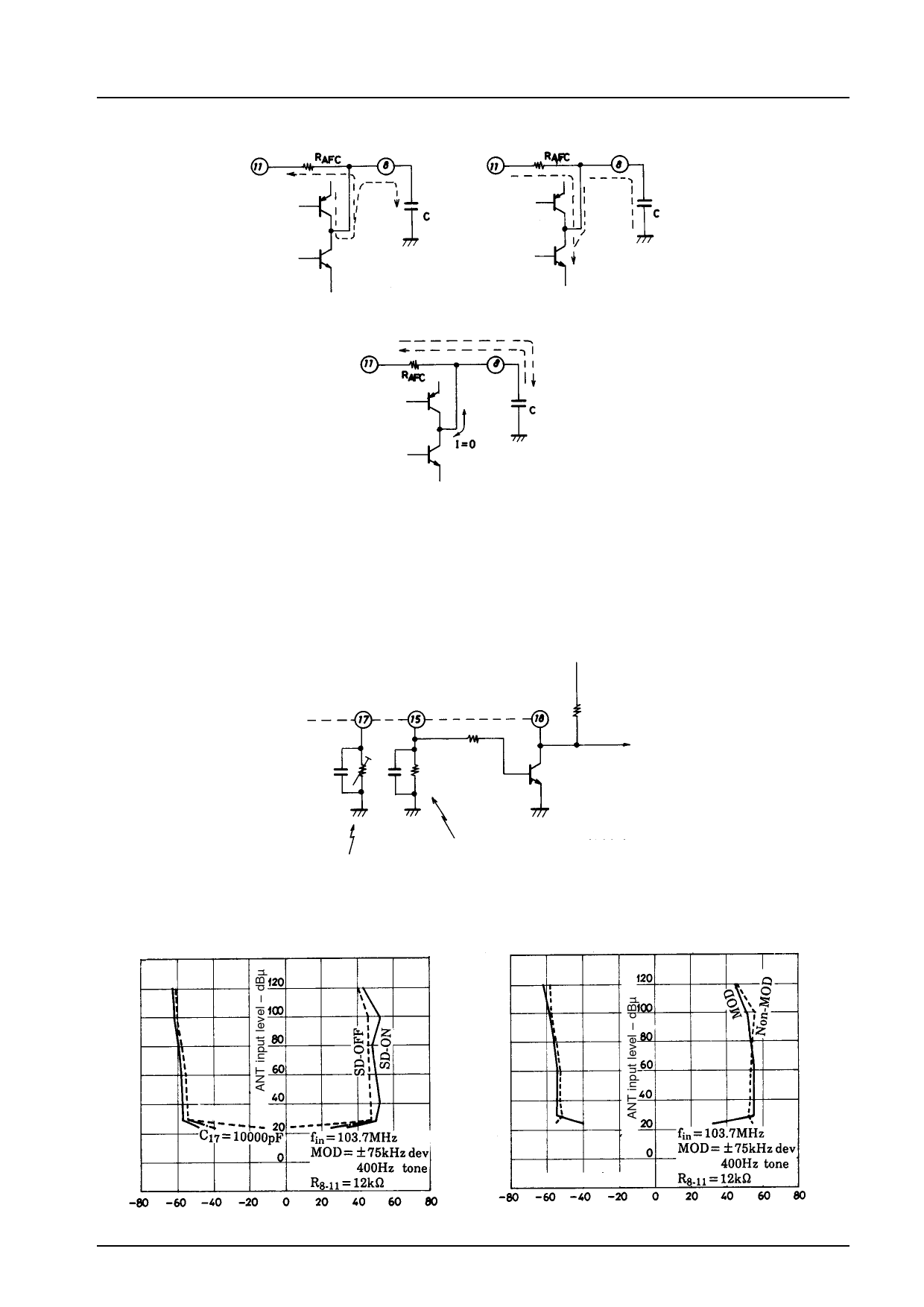
1) Current path during detuning
LA1145, 1145M
2) Current return path from detuning
The input/output current from pin 8 becomes zero during return.
As can be seen from the above circuit diagrams, the time constant during detuning is determined by the internal PNP
resistance, the NPN collector resistance and the capacitance of the externally- mounted capacitor. This time constant is
determined by the external resistance RAFC and capacitor C. This time constant, τ = RAFC × C, must be set depending on the
required search time.
3. Narrow-band SD output circuit
An IF count circuit is provided for equipment compatibility for the European marketplace. However, if the band is made
narrow using only the SD circuit, there is a tendency for the number of erroneous stops caused by an undesired signal to
increase. To prevent this, two threshold voltages should be used to control the SD circuit.
SD output
SD sensitivity setting
Mute driver pin for the 2nd threshold voltage.
Band Mute Characteristics (1)
Band Mute Characteristics (2)
Without C17
Frequency, ∆f – kHz
With C17 = 10000 pF
Frequency, ∆f – kHz
No. 2725-10/17
Share Link: 