MC74HC174ADTR2G_12 데이터 시트보기 (PDF) - ON Semiconductor
부품명
상세내역
일치하는 목록
MC74HC174ADTR2G_12 Datasheet PDF : 10 Pages
| |||
MC74HC174A
Hex D Flip-Flop with
Common Clock and Reset
High−Performance Silicon−Gate CMOS
The MC74HC174A is identical in pinout to the LS174. The device
inputs are compatible with standard CMOS outputs; with pullup
resistors, they are compatible with LSTTL outputs.
This device consists of six D flip−flops with common Clock and
Reset inputs. Each flip−flop is loaded with a low−to−high transition of
the Clock input. Reset is asynchronous and active−low.
Features
• Output Drive Capability: 10 LSTTL Loads
• Outputs Directly Interface to CMOS, NMOS, and TTL
• Operating Voltage Range: 2.0 to 6.0 V
• Low Input Current: 1.0 mA
• In Compliance with the Requirements Defined by JEDEC Standard
No. 7 A
• Chip Complexity: 162 FETs or 40.5 Equivalent Gates
• NLV Prefix for Automotive and Other Applications Requiring
Unique Site and Control Change Requirements; AEC−Q100
Qualified and PPAP Capable
• These Devices are Pb−Free, Halogen Free/BFR Free and are RoHS
Compliant
http://onsemi.com
16
1
16
1
16
1
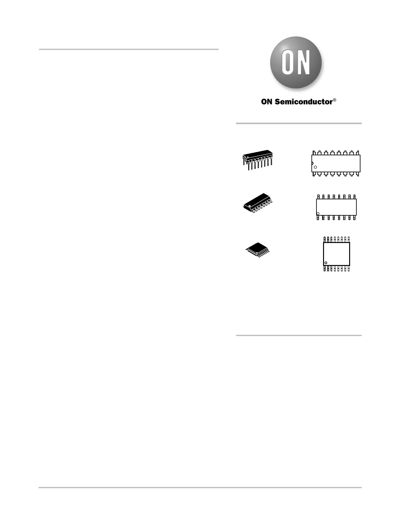
MARKING
DIAGRAMS
16
PDIP−16
N SUFFIX
CASE 648
MC74HC174AN
AWLYYWWG
1
16
SOIC−16
D SUFFIX
CASE 751B
HC174AG
AWLYWW
1
16
TSSOP−16
DT SUFFIX
CASE 948F
HC
174A
ALYWG
G
1
A
L, WL
Y, YY
W, WW
G or G
= Assembly Location
= Wafer Lot
= Year
= Work Week
= Pb−Free Package
(Note: Microdot may be in either location)
ORDERING INFORMATION
See detailed ordering and shipping information in the package
dimensions section on page 2 of this data sheet.
© Semiconductor Components Industries, LLC, 2012
1
July, 2012 − Rev. 12
Publication Order Number:
MC74HC174A/D
Share Link: 