7CE12Z 데이터 시트보기 (PDF) - NXP Semiconductors.
부품명
상세내역
일치하는 목록
7CE12Z Datasheet PDF : 21 Pages
| |||
NXP Semiconductors
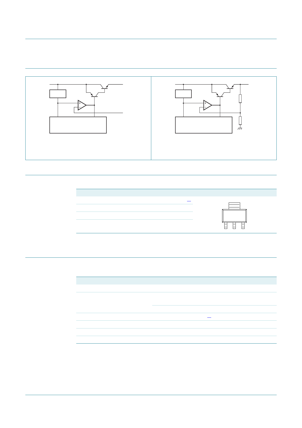
6. Functional diagram
NX1117C; NX1117CE series
Low-dropout linear regulators
VIN
Vref
VOUT
VIN
Vref
VOUT
ADJ
OUTPUT CURRENT LIMITING
SOA CONTROL
THERMAL SHUTDOWN
006aac638
Fig 1. Adjustable output voltage versions:
functional diagram
7. Pinning information
OUTPUT CURRENT LIMITING
SOA CONTROL
THERMAL SHUTDOWN
GND
006aac639
Fig 2. Fixed output voltage versions:
functional diagram
Table 4.
Pin
1
2
3
4
Pinning
Symbol
ADJ or GND
VOUT
VIN
VOUT
Description
adjust or ground
output
input
output
Simplified outline
[1]
4
123
[1] ADJ for NX1117CADJZ and NX1117CEADJZ; GND for all other devices.
8. Limiting values
Table 5. Limiting values
In accordance with the Absolute Maximum Rating System (IEC 60134).
Symbol Parameter
Conditions
Min
Max
Vin
input voltage
-
20
VESD
electrostatic discharge MIL-STD-883
2
-
voltage
(human body model)
machine model
400
-
Ptot
total power dissipation
[1] internally limited
Tj
Tamb
Tstg
junction temperature
ambient temperature
storage temperature
-
150
40
+125
65
+150
[1]
The maximum package power dissipation is
Ptot
=
T----j---–----T----a---m---b- .
Rthj – a
Unit
V
kV
V
C
C
C
NX1117C_NX1117CE_SER
Product data sheet
All information provided in this document is subject to legal disclaimers.
Rev. 2 — 11 December 2012
© NXP B.V. 2012. All rights reserved.
3 of 21
Share Link: 