L4938E 데이터 시트보기 (PDF) - STMicroelectronics
부품명
상세내역
일치하는 목록
L4938E Datasheet PDF : 12 Pages
| |||
L4938E - L4938ED - L4938EPD
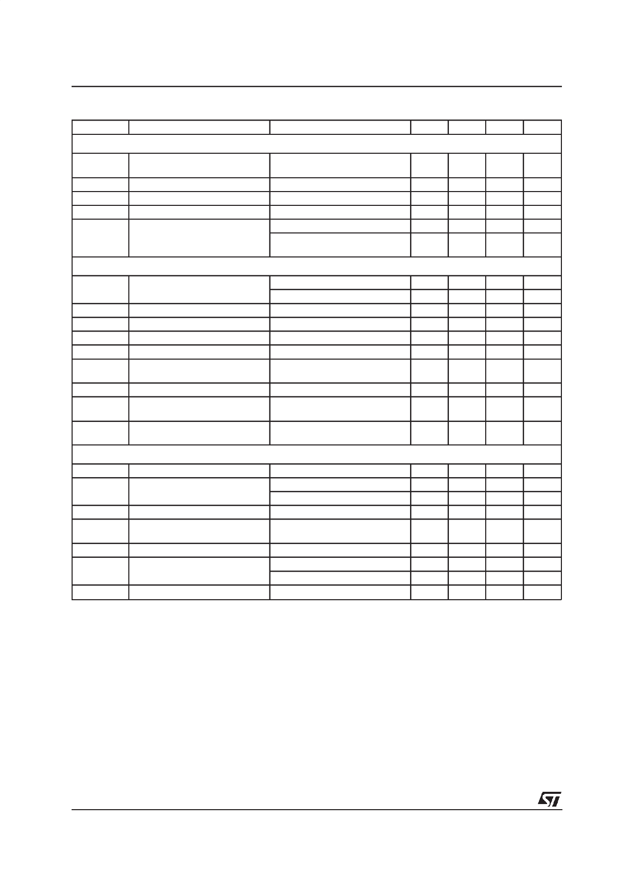
ELECTRICAL CHARACTERISTICS (Continued)
Symbol
Parameter
Test Condition
Min. Typ. Max. Unit
ENABLE INPUT
VENL
Enable Input Low Voltage
(Output 2 Active)
VENH
VENhyst
IEN LOW
IEN HIGH
Enable Input High Voltage
Enable Hysteresis
Enable Input Current Low
Enable Input Current High
VEN = 0
VEN = 1.1 to 7V; TJ < 130°C;
VEN = 1.1 to 7V;
TJ = 130 to 150°C;
-20
1
V
1.4
20
V
20
30
60
mV
-20
-8
-3
µA
-1
0
1
µA
-10
0
10
µA
RESET CIRCUIT
VRT
Reset Theresold Voltage
(note4)
VRTH
tRD min
tRD nom
tRR
ICT
ICT
VRESL
Reset Theresold Hysteresis
Reset Pulse Delay
Reset Pulse Delay
Reset Reaction Time
Pull Down Capability of the
Discharge circuit
Charge Current
Reset Output Low Voltage
VRESH
Reset Output High Leakage
current
RPR = ∞
4.5 VO1-0.3 VO1-0.2 V
RPR = 0
3.65 3.8 3.95
V
RPR = ∞
30
60
120 mV
CRES = 47nF; t r ≤ 30µs; (note 5) 40
60
100
ms
CRES = 47nF; (note 6)
60
100 140
ms
CRES = 47nF
10
50
150
µs
VOUT1 < VRT
3
6
15
mA
VOUT1 > VRT
RRES = 10KΩ to VOUT1
VOUT1 ≥ 1.5V
VRES = 5V
-1.3
-1
0.7
µA
0.4
V
1
µA
SENSE COMPARATOR
VSI
Functional Range
VSIT
Sense Threshold Voltage
VSITH
VSOL
ISOH
ISI HIGH
Sense Threshold Hysteresis
Sense Output Low Voltage
Sense Output Leakage
Sense Input Current High
ISI LOW Sense Input Current Low
-20
20
V
Falling Edge; TJ <130°C
1.08 1.16 1.24
V
Falling Edge; TJ <130 to 150°C 1.05 1.16 1.29
V
10
30
60
mV
V SI ≤ 1.05V; RSO =10KΩ
connected to 5V; VS ≥ 5V
0.4
V
VSO = 5V; VSI ≥ 1.5V
1
µA
VSI = 1.1 to 7V; TJ <130°C
-1
0
1
µA
VSI = 1.1 to 7V; TJ <130 to 150°C -10
0
10
µA
VSI = 0V
-20
-8
-3
µA
Note :
4) The reset threshold can be programmed continuously from typ 3.8V to 4.7V by changing a value of an external resistor from pin PR to GN
5) This is a minimum reset time according to the hysteresis of the comparator. Delay time starts with VOUT1 exceeding VRT
6) This is the nominal reset time depending on the discharging limit of CT (saturation voltage) and theupper threshold of the timer comparator.
Delay time starts with VOUT1 exceeding VRT
7) The leakage of CT must be less than 0.5mA (2V). If an external resistor between CT and VOUT1 is applied, the leakage current may be
increased. The external resistor should have more than 30KΩ.
for stability: Cs ≥ 1µF, C01 ≥ 10µF, C02 ≥ 10µF, ESR ≤ 5Ω (designed target) For details see application note.
8) For transients exceeding 20V or -20V external protection is required at the Pins SI and EN as shown at Pin EN. The protection proposed will
provide proper function for transients in the range of ±200V. If the zener diode is omitted the external resistor should be raised to 200KΩ
to limit the current to 1mA. Without the zener diode, the function 20V or -20V can not be guaran teed.
4/12
Share Link: 