ML7029 데이터 시트보기 (PDF) - LAPIS Semiconductor Co., Ltd.
부품명
상세내역
일치하는 목록
ML7029 Datasheet PDF : 29 Pages
| |||
FEDL7029-04
ML7029
FUNCTIONAL DESCRIPTION
Control Registers
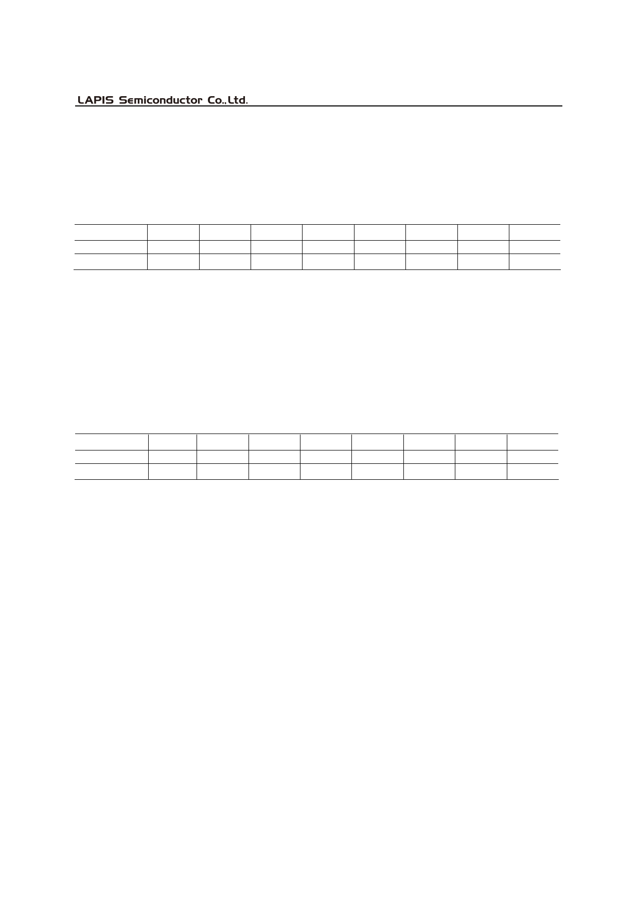
(1) CR0 (Basic operating mode setting)
B7
B6
B5
B4
B3
B2
B1
B0
CR0
—
—
PDN ALL
—
—
—
—
—
Initial Value
*
*
0
*
*
*
*
*
Note: Initial Value: Reset state by PDN (*: Don’t care)
B7, B6, B4 to B0: Not used (These pins are used to test the device. They should be set to “0” during normal
operation.)
B5:
Power-down (entire system); 0/Power-on, 1/Power-down
0 Red with the inverted external power-down signals.
When using this data, set the RDN pin to “1”.
(2) CR1 (ADPCM operating mode setting)
B7
B6
B5
B4
B3
B2
B1
CR1
MODE1 MODE0 TX RESET RX RESET TX MUTE RX MUTE
—
Initial Value
0
0
0
0
0
0
*
B0
RX PAD
0
B7, B6:
ADPCM data compression algorithm select (output bit select);
(0, 0): 4-bit output (32 kbps)
(0, 1): 8-bit output (64 kbps)
(1, 0): 3-bit output (24 kbps)
(1, 1): 2-bit output (16 kbps)
Data rates in parentheses: when SYNC = 8 kHz
B5: ADPCM of transmit reset (specified by G.726); 1/Reset*
B4: ADPCM of receive reset (specified by G.726); 1/ Reset*
B3: ADPCM transmit data mute;
1/Mute
B2: ADPCM receive data mute;
1/Mute
B1: Not used (This pin is used to test the device. It should be set to “0” during normal operation.
B0: Receive side PAD;
1/inserted in the receive side voice path, 12 dB loss
0/no PAD
* The reset width should be 1/f sample s or more.
The transmit and receive sides cannnot be reset separately.
They must be reset at the same time.
16/29
Share Link: 