MT8804A 데이터 시트보기 (PDF) - Zarlink Semiconductor Inc
부품명
상세내역
일치하는 목록
MT8804A Datasheet PDF : 9 Pages
| |||
CMOS MT8804A
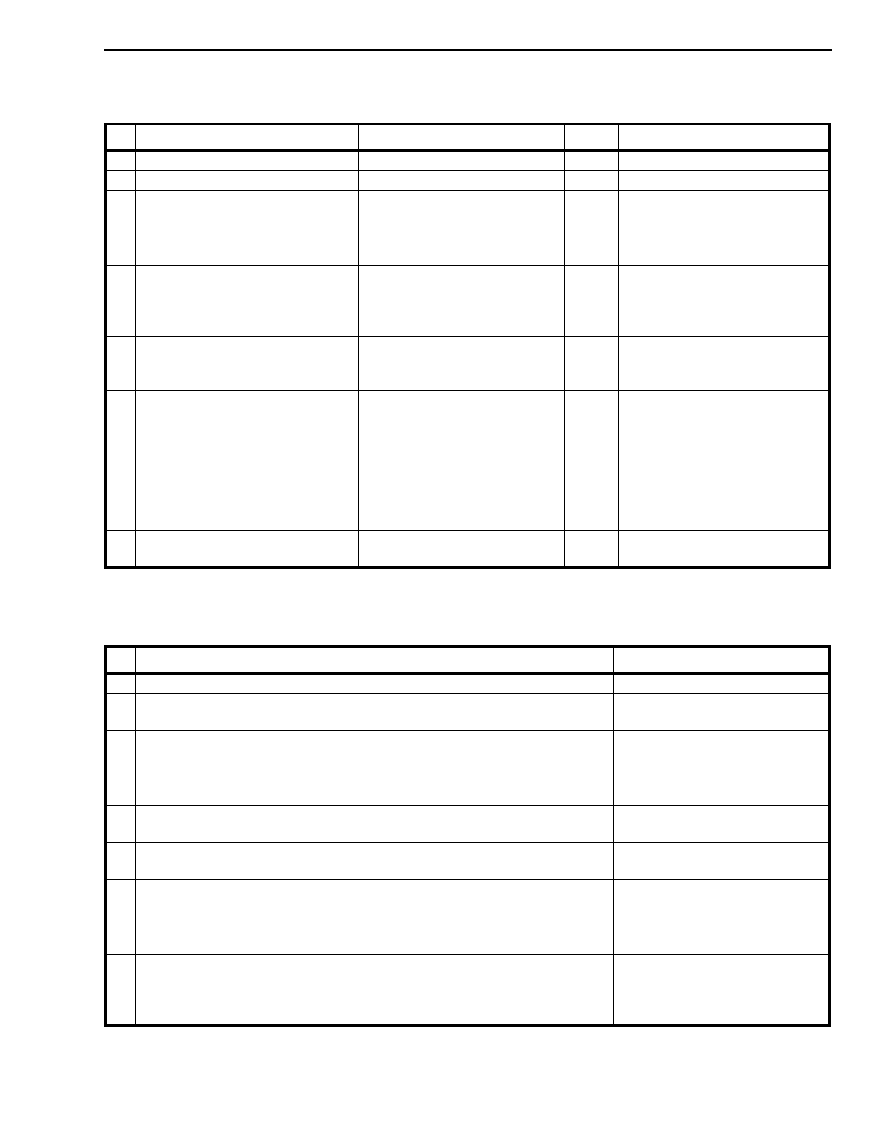
AC Electrical Characteristics† - Crosspoint Performance -VDC is the external DC offset applied at the analog
I/O pins. Voltages are with respect to VDD=10V, VSS=VEE=0V unless otherwise stated.
Characteristics
Sym Min Typ‡ Max Units
Test Conditions
1 Switch Line Capacitance
CIS
5
2 Switch Junctor Capacitance
COS
20
3 Feedthrough Capacitance
CI
0.2
4 Frequency Response
Channel “ON”
F3dB
40
20LOG(VOUT / VINA) = -3dB
5 Total Harmonic Distortion
THD
VDD=15V/VDC=7.5V
0.1
VDD=10V/VDC=5V
0.2
VDD=5V/VDC=2.5V
1.0
6 Feedthrough
FDT
-50
Channel “OFF”
Feed.=20LOG (VOUT / VINA)
7 Crosstalk between any two
Xtalk
-40
channels for switches Li - Ji and
Lj - Jj.
-90
Li - Ji is “ON“
Lj - Jj is “OFF“
pF
pF
pF
MHz
%
%
%
dB
dB
dB
Xtalk=20LOG (VJj/VLi).
8 Propagation delay through
tPS
10
ns
switch
† AC Electrical Characteristics are at ambient temperature (25°C).
‡ Typical figures are for design aid only; not guaranteed and not subject to production testing.
Switch is “ON”; VDC=5V,
VINA=5Vpp sinewave
f= 1kHz; RL = 1kΩ
Switch is “ON”; VEE=VSS=0V
VINA=5Vpp sinewave
f= 1kHz;
RL = 10kΩ
All Switches “OFF”; VINA=
5Vpp sinewave f= 1MHz;
RL= 1kΩ. VDC=5V
VINA=2Vpp sinewave
f= 1.0MHz; RL = 600Ω.
VINA=2Vpp sinewave
f= 3.4kHz; RL = 600Ω.
VDC = 5V
CL=50pF
AC Electrical Characteristics† - Control and I/O Timings- Voltages are with respect to VSS=VEE=0V unless
otherwise stated.
Characteristics
Sym Min Typ‡ Max Units
Test Conditions
1 Digital Input Capacitance
CDI
5
pF
2 Setup Time D0-D3 to AE
tDS 150
ns
200
ns
3 Hold Time D0-D3 to AE
tDH 120
ns
300
ns
4 Setup Time Address to AE
tAS
0
ns
50
ns
5 Hold Time Address to AE
tAH 120
ns
300
ns
6 AE Pulse Width
tAEW 100
ns
250
ns
7 AE to Switch Status Delay
tPAE
200 300 ns
650 900 ns
8 DATA to Switch Status Delay
9 MR to Switch Status Delay
tPLH
tPHL
tMR
tMRR
250 400 ns
650 1000 ns
250 400 ns
500 600 ns
200 350 ns
500 750 ns
† AC Electrical Characteristics are at ambient temperature (25°C).
‡ Typical figures are for design aid only; not guaranteed and not subject to production testing.
Note 1 RL= 10kΩ, CL=50pF
Note 2 RL= 1kΩ, CL=50pF
Digital Input rise time (tr) and fall time (tf) = 5ns.
VDD=10V
VDD=10V
VDD=5V
VDD=10V
VDD=5V
VDD=10V
VDD=5V
VDD=10V
VDD=5V
VDD=10V
VDD=5V
VDD=10V
VDD=5V
VDD=10V
VDD=5V
VDD=10V
VDD=5V
VDD=10V
VDD=5V
See Note 1
See Note 1
See Note 2
3-7
Share Link: 