NCP5666 데이터 시트보기 (PDF) - ON Semiconductor
부품명
상세내역
일치하는 목록
NCP5666 Datasheet PDF : 9 Pages
| |||
NCP5666
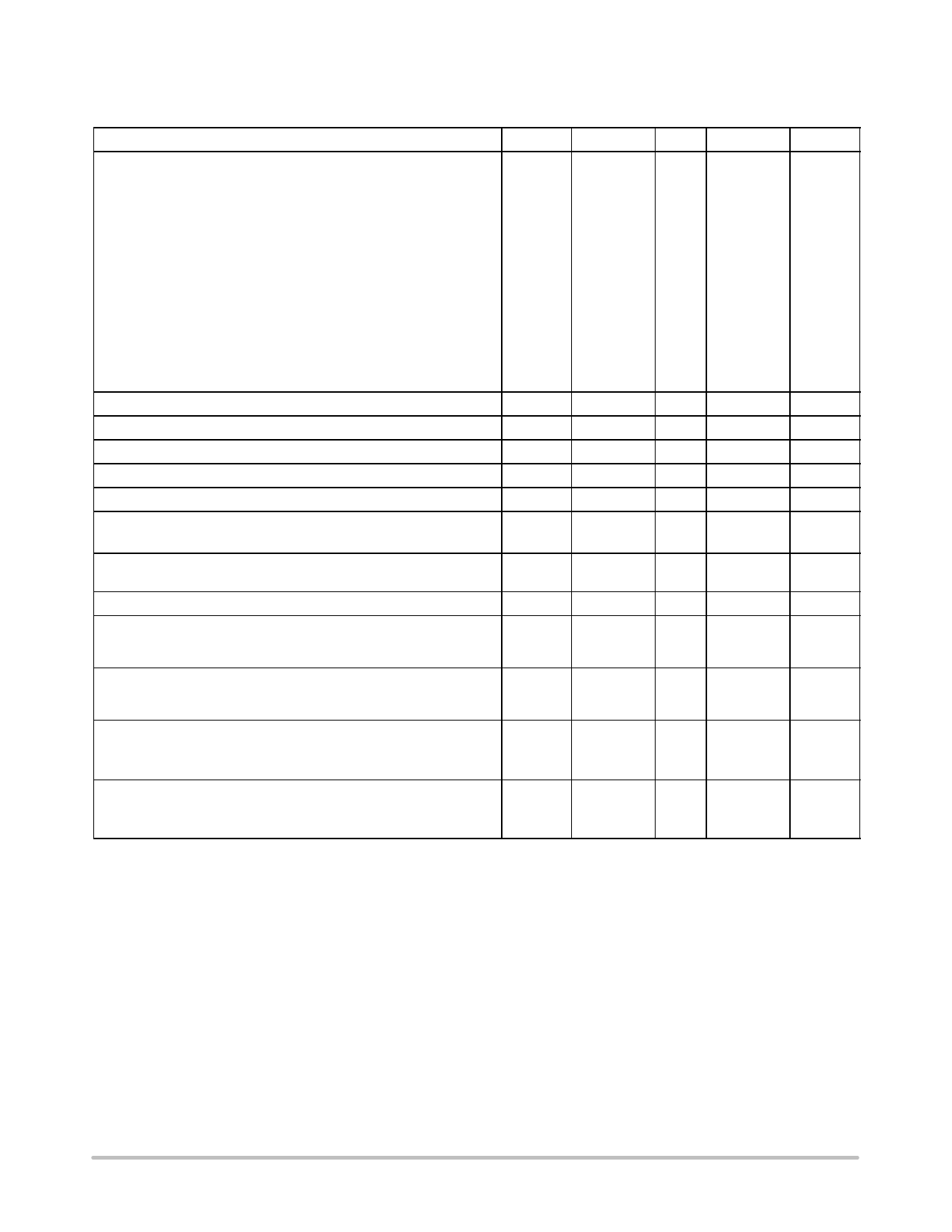
ELECTRICAL CHARACTERISTICS (Vin = Vout(nom) + 1.5 V, VEN = Vin, for typical values TA = 25°C, for min/max values TA = -40°C
to 85°C, Cin = 100 mF, Cout = 33 mF, unless otherwise noted. (Note 4))
Characteristic
Symbol
Min
Typ
Max
Unit
Output Voltage (Note 6)
2.5 V Regulator
TA = 25°C (Vin = 4.0 V to 7.0 V, Iout = 10 mA to 3.0 A)
TA = -20 to +125°C (Vin = 4.0 V to 7.0 V, Iout = 10 mA to 3.0 A)
TA = -40 to +150°C (Vin = 4.0 V to 7.0 V, Iout = 10 mA to 3.0 A)
5.0 V Regulator
TA = 25°C (Vin = 6.5 V to 7.0 V, Iout = 10 mA to 3.0 A)
TA = -20 to +125°C (Vin = 6.5 V to 7.0 V, Iout = 10 mA to 3.0 A)
TA = -40 to +150°C (Vin = 6.5 V to 7.0 V, Iout = 10 mA to 3.0 A)
Vout
V
2.475
(-1%)
2.462
(-1.5%)
2.450
(-2%)
2.500
2.500
2.500
2.525
(+1%)
2.538
(+1.5%)
2.550
(+2%)
4.950
(-1%)
4.925
(-1.5%)
4.900
(-2%)
5.000
5.000
5.000
5.050
(+1%)
5.075
(+1.5%)
5.100
(+2%)
Line Regulation (Iout = 10 mA, Vout+1.5 V < Vin < 7.0 V) (Note 5)
REGline
-
0.03
-
%
Load Regulation (10 mA < Iout < 3.0 A) (Note 5)
REGload
-
0.2
-
%
Dropout Voltage (Iout = 3.0 A)
VDO
-
1.0
1.3
V
Peak Output Current Limit
Iout
3.0
-
-
A
Internal Current Limitation (Note 5)
Ilim
-
4.5
-
A
Ripple Rejection (120 Hz) (Note 5)
Ripple Rejection (1 kHz) (Note 5)
RR
-
70
-
dB
-
65
-
Output Noise Voltage
(Vout = 2.5 V, Iout = 10 mA, Cout = 1.0 mF, f = 10 Hz to 100 kHz) (Note 5)
Thermal Shutdown (Note 5)
Ground Current (Iout = 3.0 A)
2.5 V Regulator
5.0 V Regulator
Vn
TSHD
IGND
-
57
-
mVrms
-
160
-
°C
mA
-
1.8
3.0
-
2.4
3.0
Disable Current
2.5 V Regulator
5.0 V Regulator
IDIS
mA
-
50
300
-
10
300
Enable Input Threshold Voltage
Ven
V
Voltage Increasing, On state, Logic High
1.3
-
-
Voltage Decreasing, Off state, Logic Low
-
-
0.3
Enable Input Current (Note 5)
Ien
Enable Pin Voltage = 0.3 Vmax
-
0.5
-
mA
Enable Pin Voltage = 1.3 Vmin
-
0.5
-
4. Performance guaranteed over specified operating conditions by design, guard banded test limits, and/or characterization, production tested at
TJ = TA = 25°C. Low duty cycle pulse techniques are used during testing to maintain the junction temperature as close to ambient as possible.
5. Typical values are based on design and/or characterization.
6. Other fixed output voltages available at 0.9 V, 1.2 V, 1.5 V, 1.8 V, 3.0 V, 3.3 V per request.
http://onsemi.com
4
Share Link: 