AD7450ARZ 데이터 시트보기 (PDF) - Analog Devices
부품명
상세내역
일치하는 목록
AD7450ARZ Datasheet PDF : 22 Pages
| |||
AD7450
ABSOLUTE MAXIMUM RATINGS1
(TA = 25°C, unless otherwise noted.)
VDD to GND . . . . . . . . . . . . . . . . . . . . . . . . . . –0.3 V to +7 V
VIN+ to GND . . . . . . . . . . . . . . . . . . . . –0.3 V to VDD + 0.3 V
VIN– to GND . . . . . . . . . . . . . . . . . . . . –0.3 V to VDD + 0.3 V
Digital Input Voltage to GND . . . . . . . . –0.3 V to VDD + 0.3 V
Digital Output Voltage to GND . . . . . –0.3 V to VDD + 0.3 V
VREF to GND . . . . . . . . . . . . . . . . . . . . –0.3 V to VDD + 0.3 V
Input Current to Any Pin Except Supplies2 . . . . . . . ± 10 mA
Operating Temperature Range
Commercial (A and B Version) . . . . . . . . . –40oC to +85oC
Storage Temperature Range . . . . . . . . . . . . –65oC to +150oC
Junction Temperature . . . . . . . . . . . . . . . . . . . . . . . . . . 150oC
SOIC, µSOIC Package, Power Dissipation . . . . . . . . 450 mW
JA Thermal Impedance . . . . . . . . . . . . . . . . 157°C/W (SOIC)
. . . . . . . . . . . . . . . . . . . . . . . . . . . 205.9°C/W (µSOIC)
JC Thermal Impedance . . . . . . . . . . . . . . . . . 56°C/W (SOIC)
. . . . . . . . . . . . . . . . . . . . . . . . . . . 43.74°C/W (µSOIC)
Lead Temperature, Soldering
Vapor Phase (60 secs) . . . . . . . . . . . . . . . . . . . . . . . . 215oC
Infrared (15 secs) . . . . . . . . . . . . . . . . . . . . . . . . . . . . 220oC
ESD . . . . . . . . . . . . . . . . . . . . . . . . . . . . . . . . . . . . . . . . 3.5 kV
NOTES
1Stresses above those listed under the Absolute Maximum Ratings may cause
permanent damage to the device. This is a stress rating only and functional
operation of the device at these or any conditions above those listed in the
operational sections of this specification is not implied. Exposure to absolute
maximum rating conditions for extended periods may affect device reliability.
2Transient currents of up to 100 mA will not cause SCR latch up.
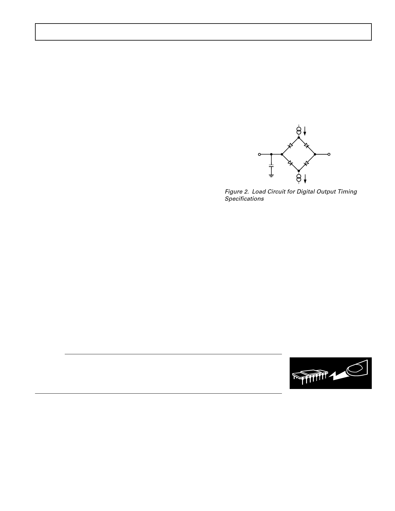
200A
IOL
TO
OUTPUT
PIN
CL
50pF
200A
IOH
1.6V
Figure 2. Load Circuit for Digital Output Timing
Specifications
CAUTION
ESD (electrostatic discharge) sensitive device. Electrostatic charges as high as 4000 V readily
accumulate on the human body and test equipment and can discharge without detection. Although the
AD7450 features proprietary ESD protection circuitry, permanent damage may occur on devices
subjected to high-energy electrostatic discharges. Therefore, proper ESD precautions are recommended to
avoid performance degradation or loss of functionality.
WARNING!
ESD SENSITIVE DEVICE
Rev. A
–5–
Share Link: 