HT7610 데이터 시트보기 (PDF) - Holtek Semiconductor
부품명
상세내역
일치하는 목록
HT7610 Datasheet PDF : 12 Pages
| |||
HT761X
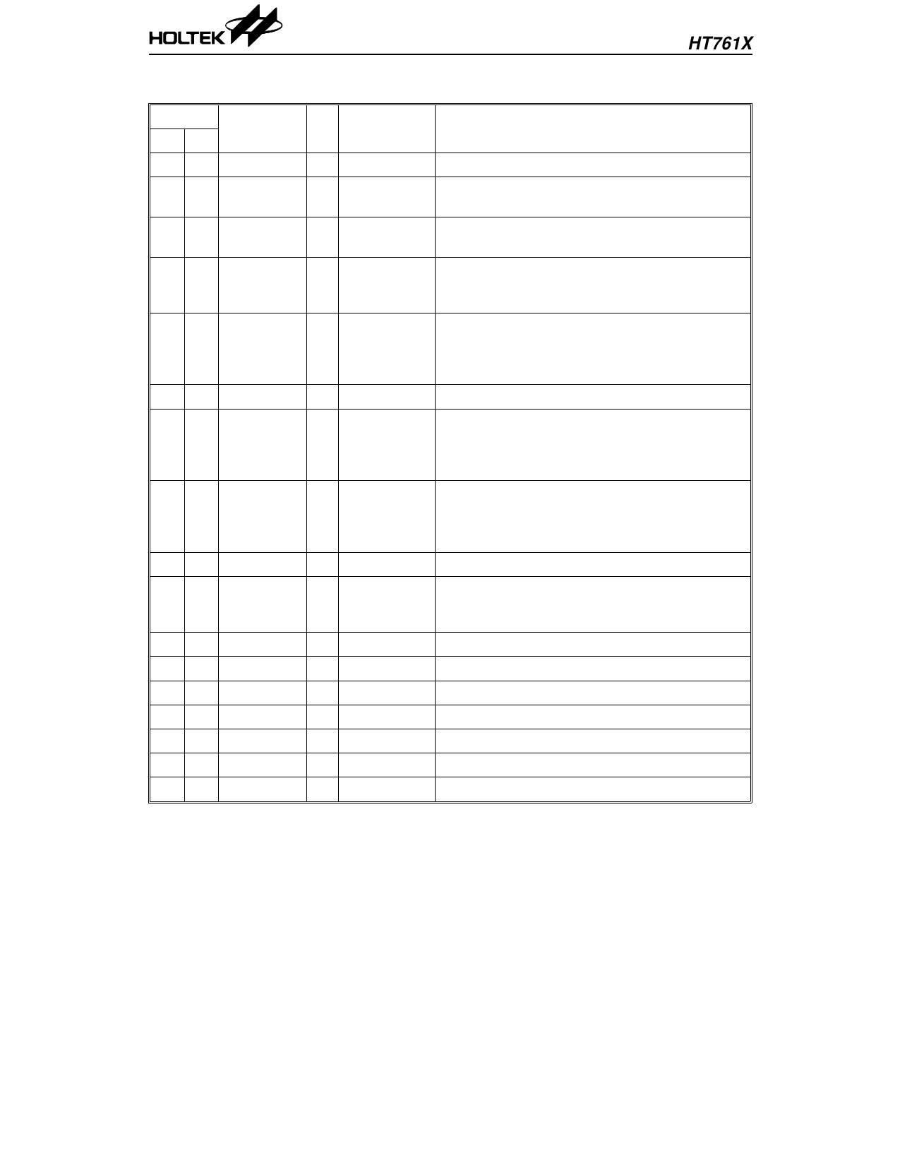
Pin Description
Pin No.
AB
11
2
2
33
44
55
66
77
88
99
10 10
11 11
12 12
13 13
14 14
15 15
16 16
Pin Name
I/O
Internal
Connection
Description
VSS
RELAY
TRIAC
OSCD
OSCS
ZC
CDS
MODE
VDD
VEE
RSTB
OP1P
OP1N
OP1O
OP2P
OP2N
OP2O
I
—
Negative power supply
O
CMOS
RELAY drive output through an external NPN
transistor, active high
O
CMOS
TRIAC drive output
The output is a pulse output when active.
I/O
PMOS IN
NMOS OUT
Output timing oscillator I/O
It is connected to an external RC to adjust output
duration.
System oscillator I/O
I/O
PMOS IN
NMOS OUT
OSCS is connected to an external RC to set the
system frequency. The system frequency ≅ 16KHz
for normal application.
I
CMOS Input for AC zero crossing detection
CDS is connected to a CDS voltage divider for
I
CMOS
daytime/night auto-detection. Low input to this pin
can disable the PIR input. CDS a schmitt trigger
input with 5-second input debounce time.
Operating mode selection input:
I
CMOS
VDD: Output is always ON
VSS: Output is always OFF
Open: Auto detection
I
—
Positive power supply
Regulated voltage output
O
NMOS The output voltage is about –4V with respect to
VDD.
I Pull-High Chip reset input, active low
I
PMOS Noninverting input of OP1
I
PMOS Inverting input of OP1
O
NMOS Output of OP1
I
PMOS Noninverting input of OP2
I
PMOS Inverting input of OP2
O
NMOS Output of OP2
3
24th Mar ’97
Share Link: 