BD9486F 데이터 시트보기 (PDF) - ROHM Semiconductor
부품명
상세내역
일치하는 목록
BD9486F Datasheet PDF : 37 Pages
| |||
BD9486F
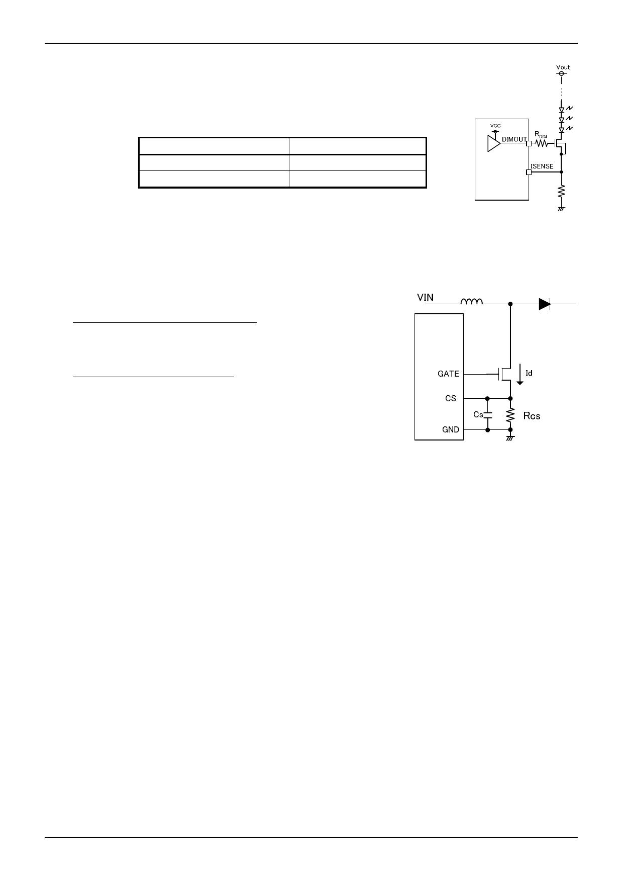
○Pin 13: DIMOUT
This is the output pin for external dimming NMOS. The table below shows the rough output
logic of each operation state, and the output H level is VCC. Please refer to “3.5 Timing Chart”
for detailed explanations, because DIMOUT logic has an exceptional behavior. Please insert
the resistor RDIM between the dimming MOS gate to improve the over shoot of LED current, as
PWM turns from low to high.
Status
Normal
Abnormal
DIMOUT output
Same logic to PWM
GND Level
Datasheet
Figure 15. DIMOUT terminal circuit example
○Pin 14: GATE
This is the output terminal for driving the gate of the boost MOSFET. The high level is VCC. Frequency can be set by the
resistor connected to RT. Refer to <RT> pin description for the frequency setting.
○Pin 15: CS
The CS pin has two functions.
1. DC / DC current mode Feedback terminal
The inductor current is converted to the CS pin voltage by the sense resistor
RCS. This voltage compared to the voltage set by error amplifier controls the
output pulse.
2. Inductor current limit (OCP) terminal
The CS terminal also has an over current protection (OCP). If the voltage is
more than 0.4V(typ.), the switching operation will be stopped compulsorily. And
the next boost pulse will be restarted to normal frequency.
In addition, the CS voltage is more than 1.0V(typ.) during four GATE clocks, IC
will be latch off. As above OCP operation, if the current continues to flow
nevertheless GATE=L because of the destruction of the boost MOS, IC will
stops the operation completely.
Both of the above functions are enabled after 300ns (typ) when GATE pin Figure 16. CS terminal circuit example
asserts high, because the Leading Edge Blanking function (LEB) is included
into this IC to prevent the effect of noise.
Please refer to section “3.3.1 OCP Setting / Calculation Method for the Current Rating of DCDC Parts”, for detailed
explanation.
If the capacitance Cs in the right figure is increased to a micro order, please be careful that the limited value of NMOS
drain current Id is more than the simple calculation. Because the current Id flows not only through Rcs but also through
Cs, as the CS pin voltage moves according to Id.
○Pin 16: VCC
This is the power supply pin of the IC. Input range is from 9V to 18V.
The operation starts at more than 7.5V(typ) and shuts down at less than 7.2V(typ)
www.rohm.com
© 2013 ROHM Co., Ltd. All rights reserved.
TSZ22111・15・001
11/34
TSZ02201-0F1F0C100240-1-2
13.Feb.2014 Rev.004
Share Link: 