AD62384AP 데이터 시트보기 (PDF) - Toshiba
부품명
상세내역
일치하는 목록
AD62384AP Datasheet PDF : 8 Pages
| |||
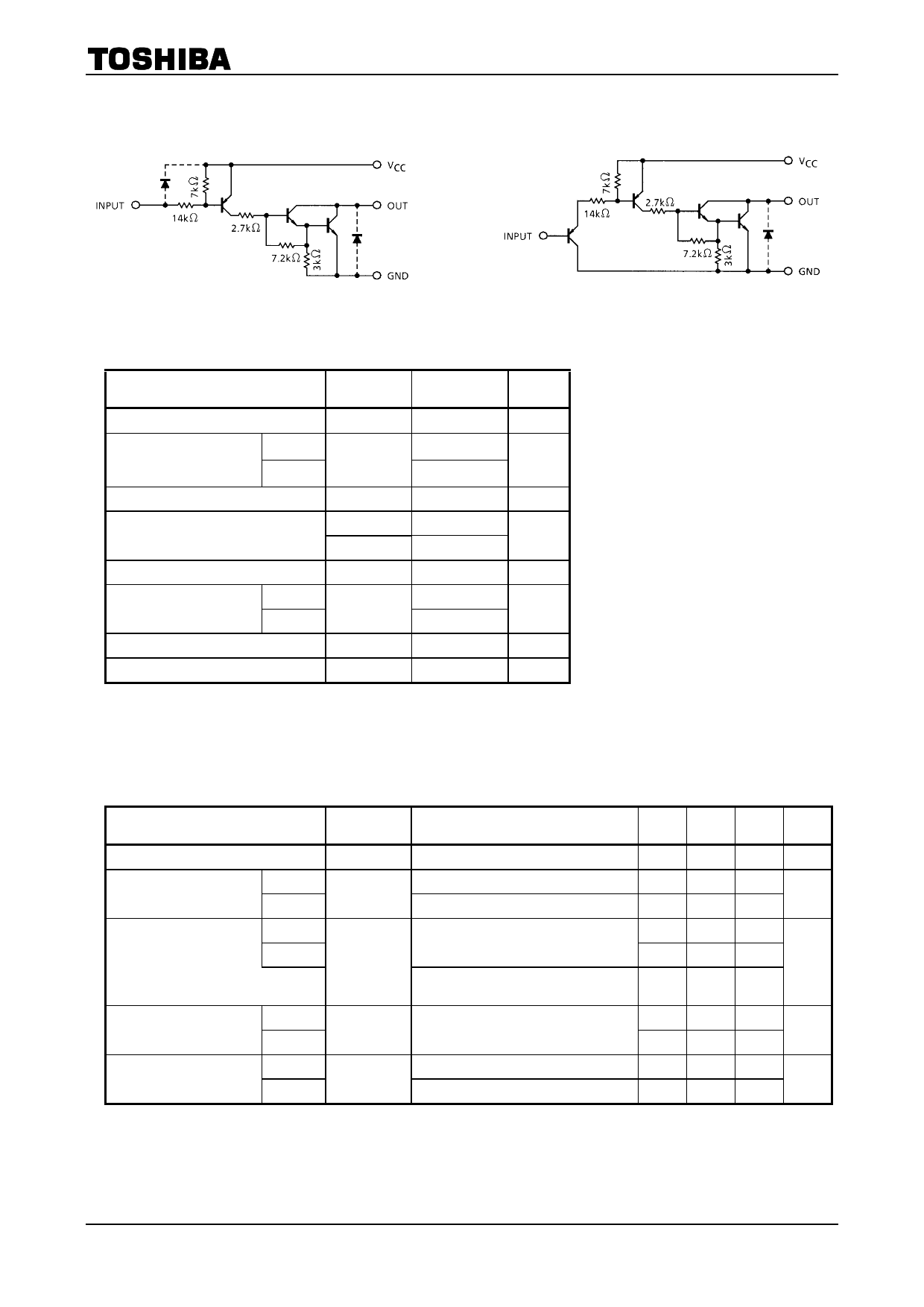
SCHEMATICS (EACH DRIVER)
TD62384AP / F / AF
TD62384,385AP/F/AF
TD62385AP / F / AF
Note : The input and output parasitic diodes cannot be used as clamp diodes.
MAXIMUM RATINGS (Ta = 25°C)
CHARACTERISTIC
SYMBOL
RATING
UNIT
Supply Voltage
Output Sustaining Voltage
Output Current
Input Voltage
Input Current
Power Dissipation
Operating Temperature
Storage Temperature
AP / AF
F
AP
F / AF
VCC
−0.5~7.0
V
−0.5~50
VCE (SUS)
V
−0.5~35
IOUT
VIN (Note 1)
VIN (Note 2)
IIN
PD (Note 3)
500
−22~VCC + 0.5
−0.5~7
−10
1.47
0.96
mA / ch
V
mA
W
Topr
−40~85
°C
Tstg
−55~150
°C
Note 1: TD62384AP / AF / F
Note 2: TD62385AP / AF / F
Note 3: Delated above 25°C in the proportion of 11.7 mW / °C (AP−Type), 7.7 mW / °C (F, AF−Type).
RECOMMENDED OPERATING CONDITIONS (Ta = −40~85°C)
CHARACTERISTIC
SYMBOL
CONDITION
Supply Voltage
Output Sustaining Voltage
Output Current
AP / AF
F
AP
F / AF
Input Voltage
Power Dissipation
TD62384
TD62385
AP
F / AF
VCC
VCE (SUS)
IOUT
VIN
PD
―
―
―
Tpw = 25 ms, Duty = 50%
8 Circuits, Ta = 85°C, Tj = 120°C
Tpw = 25 ms, Duty = 10%
1 Circuit
―
―
―
MIN TYP. MAX UNIT
4.5
5.0
5.5
V
0
―
50
V
0
―
35
0
―
115
0
―
78 mA /
ch
0
―
400
−20
―
VCC
V
0
―
5.5
―
― 0.52
W
―
― 0.35
2
2001-07-16
Share Link: 