LTC3675 데이터 시트보기 (PDF) - Linear Technology
부품명
상세내역
일치하는 목록
LTC3675 Datasheet PDF : 36 Pages
| |||
LTC3675
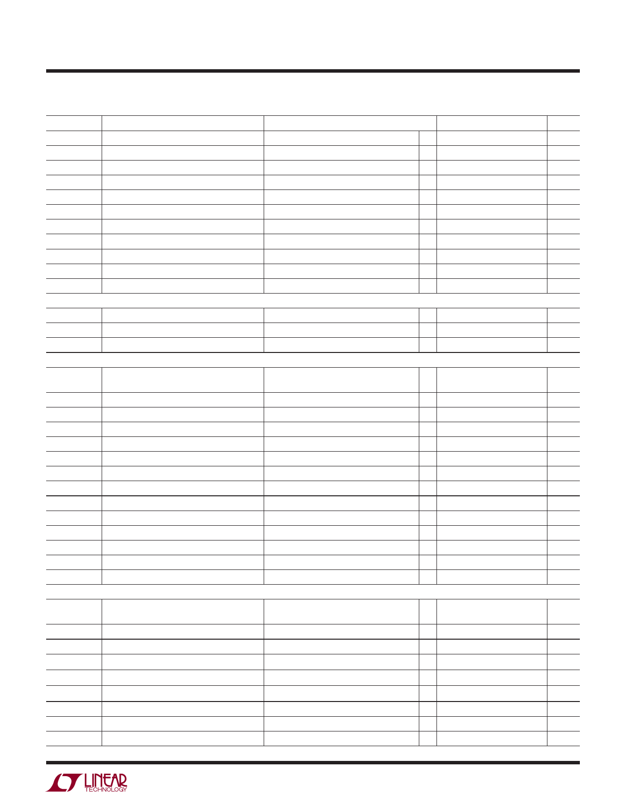
ELECTRICAL CHARACTERISTICS The l denotes the specifications which apply over the full operating
junction temperature range, otherwise specifications are at TA = 25°C. VIN = 3.6V.
SYMBOL
PARAMETER
CONDITIONS
MIN
TYP MAX UNITS
VFB3,4(HIGH) Feedback Regulation Voltage
Pulse-Skipping Mode Full-Scale (1,1,1,1) l 780
800 820
mV
VFB3,4(LOW) Feedback Regulation Voltage
Pulse-Skipping Mode Full-Scale (0,0,0,0) l 405
425 445
mV
VLSB3,4
FB3, FB4 Regulation Voltage Step Size
25
mV
IFB3,4
Feedback Leakage Current
VFB3 = VFB4 = 0.85V
–50
50
nA
DMAX3,4
Maximum Duty Cycle
VFB3 = VFB4 = 0V
l 100
%
RPMOS3,4
PMOS On-Resistance
ISW3 = ISW4 = 100mA
500
mΩ
RNMOS3,4
NMOS On-Resistance
ISW3 = ISW4 = –100mA
510
mΩ
ILEAKP3,4
PMOS Leakage Current
EN3 = EN4 = 0
–1
1
μA
ILEAKN3,4
RSWPD3,4
NMOS Leakage Current
EN3 = EN4 = 0
Output Pull-Down Resistance in Shutdown EN3 = EN4 = 0 (I2C Bit Set)
–1
1
μA
10
kΩ
tSS3,4
Soft-Start Time
500
μs
Buck Regulators Combined
IFWD1+2
PMOS Current Limit
IFWD2+3
PMOS Current Limit
IFWD3+4
PMOS Current Limit
1A Boost Regulator
FB2 = VIN (Note 6)
FB3 = VIN (Note 6)
FB4 = VIN (Note 6)
5.6
A
4
A
2.4
A
IVIN5
PWM Mode
Burst Mode Operation
VOUT5(MAX)
IFWD5
Maximum Regulated Output Voltage
Forward Current Limit
VFB5(HIGH)
VFB5(LOW)
VLSB5
IFB5
DCMAX5
RPMOS5
Feedback Regulation Voltage
Feedback Regulation Voltage
FB5 Regulation Voltage Step Size
Feedback Leakage Current
Maximum Duty Cycle
PMOS On-Resistance
RNMOS5
NMOS On-Resistance
ILEAKP
PMOS Switch Leakage Current
ILEAKN
NMOS Switch Leakage Current
ROUTPD5
Output Pull-Down Resistance in Shutdown
tSS5
Soft-Start Time
1A Buck-Boost Regulator
VFB5 = 0.85V (Notes 4, 5)
VFB5 = 0.85V (Notes 4, 5)
(Note 6)
PWM Mode Full-Scale (1,1,1,1)
PWM Mode Full-Scale (0,0,0,0)
VFB5 = 0.85V
NMOS Switch
Boost Regulator Off
150 300
μA
35
60
μA
5.35
5.55 5.75
V
2.5
3.15 3.9
A
l 780
800 820
mV
l 405
425 445
mV
25
mV
–50
50
nA
90
%
260
mΩ
275
mΩ
–2
2
μA
–2
2
μA
10
kΩ
500
μs
IVIN6
VOUT6(LOW)
VOUT6(HIGH)
IFWD6
IPEAK6
PWM Mode
Burst Mode Operation
Minimum Regulated Output Voltage
Maximum Regulated Output Voltage
Forward Current Limit
Peak Current Limit
VFB6 = 0.85V (Note 4, 5)
VFB6 = 0.85V(Note 4, 5)
PWM Mode (Note 6)
Burst Mode Operation (Note 6)
220 400
μA
20
40
μA
2.65 2.8
V
5.25
5.65
V
2.1
2.65 3.2
A
200
275 350
mA
IZERO6
VFB6(HIGH)
VFB6(LOW)
VLSB6
Zero Current Limit
Feedback Regulation Voltage
Feedback Regulation Voltage
FB6 Regulation Voltage Step Size
Burst Mode Operation
PWM Mode Full-Scale (1,1,1,1)
PWM Mode Full-Scale (0,0,0,0)
–30
0
30
mA
l 780
800 820
mV
l 405
425 445
mV
25
mV
3675f
5
Share Link: 