LA7530 데이터 시트보기 (PDF) - SANYO -> Panasonic
부품명
상세내역
일치하는 목록
LA7530 Datasheet PDF : 3 Pages
| |||
LA7530N
Operating Conditions at Ta = 25˚C
Parameter
Symbol
Recommended supply voltage
Operating voltage range
VCC
VCC op
Conditions
Ratings
Unit
12 V
9 to 13.2 V
Operating Characteristics at Ta = 25˚C, VCC=12V, fP=58.75MHz, fs=54.25MHz (VIF), fo=4.5MHz (SIF)
Parameter
Symbol
Conditions
Ratings
Unit
min
typ
max
Total circuit current
Maximum RF AGC voltage
Minimum RF AGC voltage
Quiescent video output voltage
Quiescent AFT output voltage
Input sensitivity
AGC range
Maximum allowable input
Video output amplitude
Output S/N
I17
DC
V10H DC
V10L DC
V16
DC
V11
DC
Vi
fm=400Hz, 40%AM, VO=0.8Vp-p
GR
fm=400Hz, 40%AM, VO=0.8Vp-p
Vi max fm=15kHz, 78%AM, VO=±1dB
VO(VIDEO) Vi=10mVrms, fm=15kHz, 78%AM
S/N
Vi=10mVrms CW
47
58
8.5
8.9
5.7
6.1
4.5
6.5
30
36
57
65
100 200
1.9
2.2
48
54
74 mA
9.2 V
0.5 V
6.5 V
7.5 V
42 dBµ
dB
mVrms
2.5 Vp-p
dB
Carrier leakage
CL
Vi=100mVrms, fm=15kHz, 78%AM
50
55
dB
Maximum AFT voltage
Mimimum AFT voltage
AFT detection sensitivity
V11H
V11L
Sf
Vi=10mVrms CW SWEEP
Vi=10mVrms CW SWEEP
Vi=10mVrms CW SWEEP
11 11.4
0.5
80 110
V
1.0 V
150 mV/kHz
White noise threshold level
White noise clamp level
Black noise threshold level
Black noise clamp level
SIF output signal voltage
Frequency characteristic
Differential gain
VWTH
VWCL
VBTH
VBCL
VO(SIF)
fC
DG
Vi=10mVrms SWEEP
Vi=10mVrms SWEEP
Vi=10mVrms SWEEP
Vi=10mVrms SWEEP
P/S=20dB
–3dB
Vi=–27dBm (peak) 87.5% VIDEOMOD
6.4
6.8
7.2 V
4.2
4.6
5.0 V
2.1
2.4
2.7 V
3.8
4.2
4.6 V
80 140 210 mVrms
5
7
MHz
3
%
Differential phase
DP
Vi=–27dBm (peak) 87.5% VIDEOMOD
3
deg
Input resistance
Ri
1.0
1.5
2.0 kΩ
Input capacitance
Ci
3.0
6.0 pF
SIF limiting voltage
Vi(lim) –3dB
200 500 µVrms
Detection output voltage
Total harmonic distortion
VO(DET) Vi=100mVrms, fm=400Hz, ∆f=±25kHz
THD(DET) Vi=100mVrms, fm=400Hz, ∆f=±25kHz
450 680 850 mVrms
0.5
1.3 %
AM rejection
AMR Vi=100mVrms, fm=400Hz, ∆f=±25kHz, 30% AM
50
60
dB
Usage Note : 1. Protective circuits must be inserted when using this IC with lines directly connecting the IC pins to external circuits.
(For example, this applies to pins 12 and 15.)
2. A 1000pF capacitor must be connected between either pin 5 and ground or between pin 5 and pin 8 to prevent VIF amplifier
oscillation.
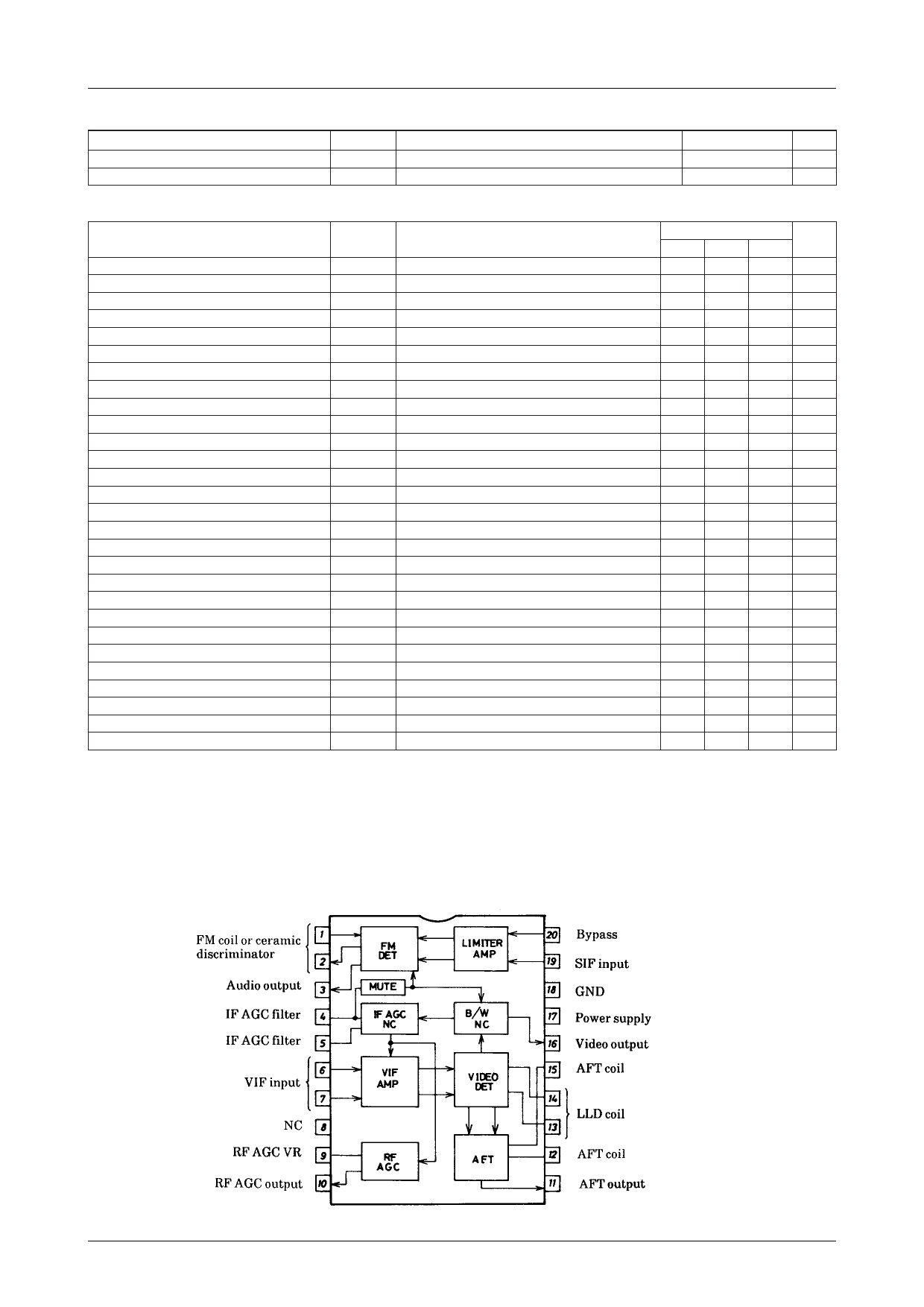
Equivalent Circuit Block Diagram
No.1774–2/3
Share Link: 