RT9266CX5 데이터 시트보기 (PDF) - Richtek Technology
부품명
상세내역
일치하는 목록
RT9266CX5 Datasheet PDF : 14 Pages
| |||
RT9266
Preliminary
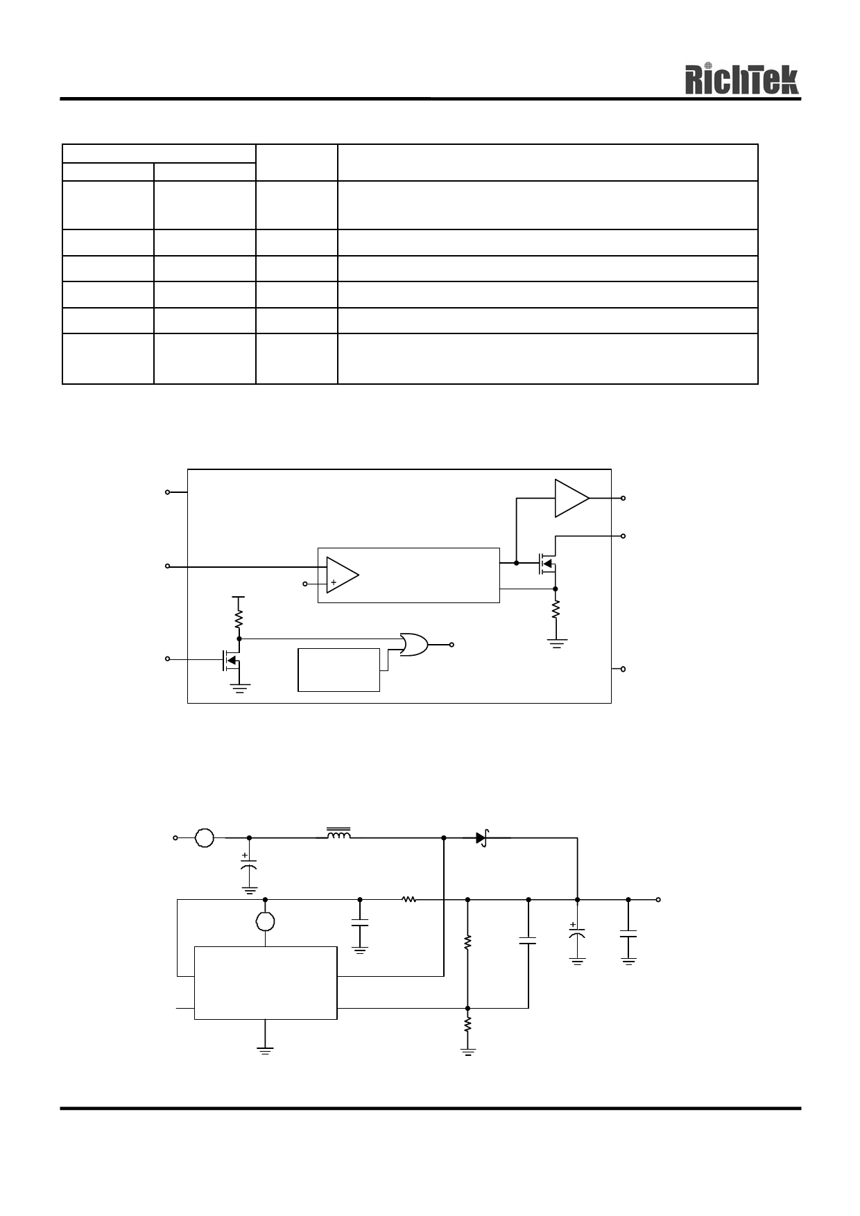
Pin Description
Pin No.
RT9266CX5 RT9266CE
1
1
2
5
3
4
4
2
5
3
6
Pin Name Pin Function
CE
EXT
GND
LX
VDD
FB
Chip enable
RT9266 gets into shutdown mode when CE pin set to low.
Output pin for driving external NMOS
Ground
Pin for switching
Input positive power pin of RT9266
Feedback input pin
Internal reference voltage for the error amplifier is 1.25V.
Function Block Diagram
VDD
FB
CE
RT9266
_
VDD 1.25 V
Loop Control Circuit
R2
Q3
Over Temp.
NMOS Detector
Shut Down
EXT
LX
Q1
NMOS
R1
GND
Test Circuit
I (VIN)
L1
VIN
A
10µH
C3
100µF
R3
A I (VDD)
C2 100
1µF
VDD
CE RT9266 LX
EXT GND
FB
D1
1N5819
R1
C4
1.6M/3M 102
C1
100µF
VOU T
3.3V/5V
C5
106
R2
980K/1M
www.richtek.com
4
DS9266-02 February 2003
Share Link: 