RT9266CE 데이터 시트보기 (PDF) - Richtek Technology
부품명
상세내역
일치하는 목록
RT9266CE Datasheet PDF : 14 Pages
| |||
RT9266
Preliminary
Application Note
Output Voltage Setting
Referring to application circuits, the output voltage of
the switching regulator (VOUT) can be set with Eq.1.
VOUT1 = (1+ R1) ×1.25V
R2
Eq.1
Feedback Loop Design
Referring to application circuits, The selection of R1
and R2 based on the trade-off between quiescent
current consumption and interference immunity is
stated below:
• Follow Eq.1
• Higher R reduces the quiescent current (Path
current = 1.25V/R2), however resistors beyond
5MΩ are not recommended.
• Lower R gives better noise immunity, and is less
sensitive to interference, layout parasitics, FB
node leakage, and improper probing to FB pins.
Layout Guide
• A full GND plane without gap break.
• VDD to GND noise bypass – Short and wide
connection for the 1µF MLCC capacitor between
Pin5 and Pin3.
• VIN to GND noise bypass – Add a capacitor close
to L1 inductor, when VIN is not an idea voltage
source.
• Minimized FB node copper area and keep far
away from noise sources.
• Minimized parasitic capacitance connecting to LX
and EXT nodes, which may cause additional
switching loss.
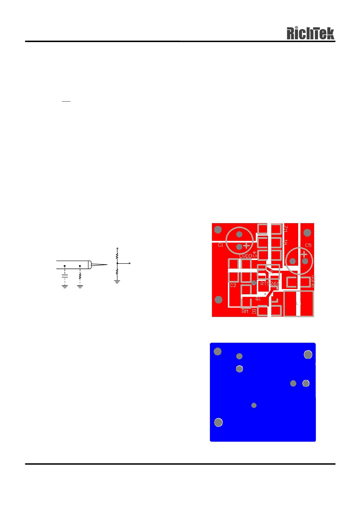
Board Layout Example (2-Layer Board)
(Refer to Application Circuit Fig. 2 for the board)
Prober Parasitics
_
Q
+
VOU T1
R1
FB Pin
R2
• A proper value of feed forward capacitor parallel
with R1 can improve the noise immunity of the
feedback loops, especially in an improper layout.
An empirical suggestion is around 0~33pF for
feedback resistors of MΩ, and 10nF~0.1µF for
feedback resistors of tens to hundreds KΩ.
For applications without standby or suspend modes,
lower values of R1 and R2 are preferred. For
applications concerning the current consumption in
standby or suspend modes, the higher values of R1
and R2 are needed. Such “high impedance feedback
loops” are sensitive to any interference, which require
careful layout and avoid any interference, e.g.
probing to FB pin.
- Top Layer –
- Bottom Layer -
www.richtek.com
10
DS9266-02 February 2003
Share Link: 